NE555N STMicroelectronics, NE555N Datasheet
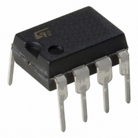
IC TIMER SINGLE BIPOLAR 8 DIP

NE555N

Manufacturer Part Number
NE555N
Description
IC TIMER SINGLE BIPOLAR 8 DIP
Manufacturer
STMicroelectronics
Type
555 Type, Timer/Oscillator (Single)r
Datasheets

Specifications of NE555N

Frequency
500kHz
Voltage - Supply
4.5 V ~ 16 V
Current - Supply
10mA
Operating Temperature
0°C ~ 70°C
Package / Case
8-DIP (0.300", 7.62mm)
Number Of Internal Timers
1
Supply Voltage (max)
16 V
Supply Voltage (min)
4.5 V
Maximum Operating Temperature
+ 70 C
Minimum Operating Temperature
0 C
Mounting Style
Through Hole
Current, Supply
3 mA (Typ.)
Number Of Pins
8
Package Type
DIP
Temperature, Operating
0 °C
Temperature, Storage
-65 to +150 °C
Time, Fall, Output
100 ns (Typ.)
Time, Rise, Output
100 ns (Typ.)
Voltage, Control
10 V (Typ.)
Voltage, Output, High Level
12.5 V (Typ.) @ 200 mA
Voltage, Output, Low Level
2.5 V (Typ.) @ 200 mA
Voltage, Supply
4.5 to 16 V
Lead Free Status / RoHS Status
Lead free / RoHS Compliant
Count
-
Lead Free Status / Rohs Status
Lead free / RoHS Compliant
Other names
497-1963-5

Available stocks

Company
Part Number
Manufacturer
Quantity
Price
Part Number:
NE555N
Manufacturer:
STE
Quantity:
7 250
Part Number:
NE555N
Manufacturer:
ST
Quantity:
12
Part Number:
NE555N
Manufacturer:
ST
Quantity:
9
Part Number:
NE555N
Manufacturer:
ST101
Quantity:
431
Part Number:
NE555N
Manufacturer:
PHI
Quantity:
1 000
Part Number:
NE555N
Manufacturer:
PHI
Quantity:
2 690
Part Number:
NE555N
Manufacturer:
SMT
Quantity:
20 000
Company:
Part Number:
NE555N
Quantity:
3 600
Part Number:
NE555N(P/B)
Manufacturer:
ST
0
Part Number:
NE555N(ST)
Manufacturer:
ST
0
Part Number:
NE555N-
Manufacturer:
ST
0
Part Number:
NE555N_STM
Manufacturer:
STM
Quantity:
309
DESCRIPTION
The NE555 monolithic timing circuit is a highly sta-
ble controller capable of producing accurate time
delays or oscillation. In the time delay mode of op-
eration, the time is precisely controlled by one ex-
ternal resistor and capacitor. For a stable opera-
tion as an oscillator, the free running frequency
and the duty cycle are both accurately controlled
with two external resistors and one capacitor.
The circuit may be triggered and reset on falling
waveforms, and the output structure can source or
sink up to 200mA.
ORDER CODE
N = Dual in Line Package (DIP)
D = Small Outline Package (SO) - also available in Tape & Reel (DT)
June 2003
NE555
SA555
SE555
Part Number
LOW TURN OFF TIME
MAXIMUM OPERATING FREQUENCY
GREATER THAN 500kHz
TIMING FROM MICROSECONDS TO
HOURS
OPERATES IN BOTH ASTABLE AND
MONOSTABLE MODES
HIGH OUTPUT CURRENT CAN SOURCE
OR SINK 200mA
ADJUSTABLE DUTY CYCLE
TTL COMPATIBLE
TEMPERATURE STABILITY OF 0.005%
PER°C
Temperature Range
-40°C, 105°C
-55°C, 125°C
GENERAL PURPOSE SINGLE BIPOLAR TIMERS
0°C, 70°C
Package
N
D
PIN CONNECTIONS (top view)
1 - GND
2 - Trigger
3 - Output
4 - Reset
(Plastic Micropackage)
1
2
3
4
(Plastic Package)
SA555 - SE555
SO8
D
DIP8
N
5 - Control voltage
6 - Threshold
7 - Discharge
8 - Vcc
8
7
6
5
NE555
1/9

Related parts for NE555N

NE555N Summary of contents

Page 1

GENERAL PURPOSE SINGLE BIPOLAR TIMERS LOW TURN OFF TIME MAXIMUM OPERATING FREQUENCY GREATER THAN 500kHz TIMING FROM MICROSECONDS TO HOURS OPERATES IN BOTH ASTABLE AND MONOSTABLE MODES HIGH OUTPUT CURRENT CAN SOURCE OR SINK 200mA ADJUSTABLE DUTY CYCLE TTL COMPATIBLE ...

Page 2

NE555-SA555-SE555 BLOCK DIAGRAM SCHEMATIC DIAGRAM ABSOLUTE MAXIMUM RATINGS Symbol V Supply Voltage CC T Junction Temperature j T Storage Temperature Range stg OPERATING CONDITIONS Symbol Supply Voltage Maximum Input Voltage th ...

Page 3

ELECTRICAL CHARACTERISTICS T Symbol Parameter Supply Current ( note Low Stage High State V CC Timing Error (monostable 100k , Initial Accuracy ...

Page 4

NE555-SA555-SE555 Figure 1 : Minimum Pulse Width Required for Triggering Figure 2 : Supply Current versus Supply Voltage Figure 3 : Delay Time versus Temperature 4/9 Figure 4 : Low Output Voltage versus Output Sink Current Figure 5 : Low ...

Page 5

Figure 7 : High Output Voltage Drop versus Output Figure 8 : Delay Time versus Supply Voltage Figure 9 : Propagation Delay versus Voltage Level of Trigger Value NE555-SA555-SE555 APPLICATION INFORMATION MONOSTABLE OPERATION In the monostable mode, the timer functions ...

Page 6

NE555-SA555-SE555 Figure 0 div INPUT = 2.0V/div OUTPUT VOLTAGE = 5.0V/div CAPACITOR VOLTAGE = 2.0V/div Figure ...

Page 7

PULSE WIDTH MODULATOR When the timer is connected in the monostable mode and triggered with a continuous pulse train, the output pulse width can be modulated by a sig- nal applied to pin 5. Figure 16 shows the circuit. Figure ...

Page 8

NE555-SA555-SE555 PACKAGE MECHANICAL DATA DIM. MIN 0.7 B 1. 0.44 8/9 Plastic DIP-8 MECHANICAL DATA mm. TYP MAX. MIN. 3.3 0.028 1.65 0.055 1.04 ...

Page 9

... No license is granted by implication or otherwise under any patent or patent rights of STMicroelectronics. Specifications mentioned in this publication are subject to change without notice. This publication supersedes and replaces all information previously supplied ...

Related keywords