PCF8583P/F5,112 NXP Semiconductors, PCF8583P/F5,112 Datasheet - Page 13
PCF8583P/F5,112
Manufacturer Part Number
PCF8583P/F5,112
Description
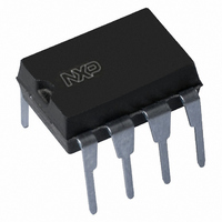
IC CLK/CALENDAR 240X8 RAM 8-DIP
Manufacturer
NXP Semiconductors
Type
Clock/Calendar/NVSRAMr
Datasheet
1.PCF8583T5518.pdf
(37 pages)
Specifications of PCF8583P/F5,112
Package / Case
8-DIP (0.300", 7.62mm)
Memory Size
240B
Time Format
HH:MM:SS (12/24 hr)
Date Format
YY-MM-DD
Interface
I²C, 2-Wire Serial
Voltage - Supply
1 V ~ 6 V
Operating Temperature
-40°C ~ 85°C
Mounting Type
Through Hole
Mounting Style
Through Hole
Lead Free Status / RoHS Status
Lead free / RoHS Compliant
Lead Free Status / RoHS Status
Lead free / RoHS Compliant, Lead free / RoHS Compliant
Other names
568-1084-5
935261345112
PCF8583PN
935261345112
PCF8583PN
Available stocks
Company
Part Number
Manufacturer
Quantity
Price
Company:

Part Number:
PCF8583P/F5,112
Manufacturer:
LTC
Quantity:
147


NXP Semiconductors
PCF8583
Product data sheet
7.10 Oscillator and divider
7.9 Interrupt output
this mode, the timer (location 07h) increments once for every one, one hundred, ten
thousand, or 1 million events, depending on the value programmed in bits 0, 1 and 2 of
the alarm control register. In all other events, the timer functions are as in the clock mode.
The conditions for activating the output INT (active LOW) are determined by appropriate
programming of the alarm control register. These conditions are clock alarm, timer alarm,
timer overflow, and event counter alarm. An interrupt occurs when the alarm flag or the
timer flag is set, and the corresponding interrupt is enabled. In all events, the interrupt is
cleared only by software resetting of the flag which initiated the interrupt.
In the clock mode, if the alarm enable is not activated (alarm enable bit of the control and
status register is logic 0), the interrupt output toggles at 1 Hz with a 50 % duty cycle (may
be used for calibration). This is the default power-on state of the device. The OFF voltage
of the interrupt output may exceed the supply voltage, up to a maximum of 6.0 V. A logic
diagram of the interrupt output is shown in
A 32.768 kHz quartz crystal has to be connected to OSCI and OSCO. A trimmer capacitor
between OSCI and V
signal is derived from the quartz oscillator for the clock counters.
Fig 13. Alarm control register, event counter mode
MSB
7
All information provided in this document is subject to legal disclaimers.
013aaa376
6
DD
Rev. 06 — 6 October 2010
is used for tuning the oscillator (see
5
4
3
2
Figure
1
Clock and calendar with 240 x 8-bit RAM
LSB
0
12.
clock alarm function:
00
01
10
11
memory location 08h
reset state: 0000 0000
000
001
010
011
100
101
110
111
timer interrupt enable:
0
1
timer function:
0
1
timer alarm enable:
0
1
alarm interrupt enable:
Section
no event alarm
event alarm
not allowed
not allowed
no timer alarm
timer alarm
no timer
units
100
10 000
1 000 000
not allowed
not allowed
test mode, all counters
in parallel
timer flag, no interrupt
timer flag, interrupt
alarm flag, no interrupt
alarm flag, interrupt
11.1). A 100 Hz clock
PCF8583
© NXP B.V. 2010. All rights reserved.
13 of 37
Related parts for PCF8583P/F5,112
Image
Part Number
Description
Manufacturer
Datasheet
Request
R

Part Number:
Description:
Manufacturer:
NXP Semiconductors
Datasheet:

Part Number:
Description:
NXP Semiconductors designed the LPC2420/2460 microcontroller around a 16-bit/32-bitARM7TDMI-S CPU core with real-time debug interfaces that include both JTAG andembedded trace
Manufacturer:
NXP Semiconductors
Datasheet:

Part Number:
Description:
NXP Semiconductors designed the LPC2458 microcontroller around a 16-bit/32-bitARM7TDMI-S CPU core with real-time debug interfaces that include both JTAG andembedded trace
Manufacturer:
NXP Semiconductors
Datasheet:
Part Number:
Description:
NXP Semiconductors designed the LPC2468 microcontroller around a 16-bit/32-bitARM7TDMI-S CPU core with real-time debug interfaces that include both JTAG andembedded trace
Manufacturer:
NXP Semiconductors
Datasheet:
Part Number:
Description:
NXP Semiconductors designed the LPC2470 microcontroller, powered by theARM7TDMI-S core, to be a highly integrated microcontroller for a wide range ofapplications that require advanced communications and high quality graphic displays
Manufacturer:
NXP Semiconductors
Datasheet:
Part Number:
Description:
NXP Semiconductors designed the LPC2478 microcontroller, powered by theARM7TDMI-S core, to be a highly integrated microcontroller for a wide range ofapplications that require advanced communications and high quality graphic displays
Manufacturer:
NXP Semiconductors
Datasheet:
Part Number:
Description:
The Philips Semiconductors XA (eXtended Architecture) family of 16-bit single-chip microcontrollers is powerful enough to easily handle the requirements of high performance embedded applications, yet inexpensive enough to compete in the market for hi
Manufacturer:
NXP Semiconductors
Datasheet:
Part Number:
Description:
The XA-S3 device is a member of Philips Semiconductors? XA(eXtended Architecture) family of high performance 16-bitsingle-chip microcontrollers
Manufacturer:
NXP Semiconductors
Datasheet:

Part Number:
Description:
The NXP BlueStreak LH75401/LH75411 family consists of two low-cost 16/32-bit System-on-Chip (SoC) devices
Manufacturer:
NXP Semiconductors
Datasheet:
Part Number:
Description:
The NXP LPC3130/3131 combine an 180 MHz ARM926EJ-S CPU core, high-speed USB2
Manufacturer:
NXP Semiconductors
Datasheet:
Part Number:
Description:
The NXP LPC3141 combine a 270 MHz ARM926EJ-S CPU core, High-speed USB 2
Manufacturer:
NXP Semiconductors
Part Number:
Description:
The NXP LPC3143 combine a 270 MHz ARM926EJ-S CPU core, High-speed USB 2
Manufacturer:
NXP Semiconductors

Part Number:
Description:
The NXP LPC3152 combines an 180 MHz ARM926EJ-S CPU core, High-speed USB 2
Manufacturer:
NXP Semiconductors
Part Number:
Description:
The NXP LPC3154 combines an 180 MHz ARM926EJ-S CPU core, High-speed USB 2
Manufacturer:
NXP Semiconductors