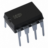
PCF8593P,112 NXP Semiconductors, PCF8593P,112 Datasheet - Page 11

PCF8593P,112
Manufacturer Part Number
PCF8593P,112
Description
IC CLOCK/CALENDAR LOW PWR 8-DIP
Manufacturer
NXP Semiconductors
Type
Clock/Calendar/NVSRAMr
Datasheet
1.PCF8593T1118.pdf
(35 pages)
Specifications of PCF8593P,112
Package / Case
8-DIP (0.300", 7.62mm)
Time Format
HH:MM:SS:hh (12/24 hr)
Date Format
YY-MM-DD-dd
Memory Size
8B
Interface
I²C, 2-Wire Serial
Voltage - Supply
1 V ~ 6 V
Operating Temperature
-40°C ~ 85°C
Mounting Type
Through Hole
Function
Clock/Calendar/Alarm/Timer Interrupt
Rtc Memory Size
8 Byte
Supply Voltage (max)
6 V
Supply Voltage (min)
1 V
Maximum Operating Temperature
+ 85 C
Minimum Operating Temperature
- 40 C
Mounting Style
Through Hole
Rtc Bus Interface
Serial (I2C)
Bus Type
Serial (I2C)
User Ram
8Byte
Package Type
PDIP
Operating Supply Voltage (max)
6V
Operating Temperature Classification
Industrial
Operating Temperature (max)
85C
Operating Temperature (min)
-40C
Pin Count
8
Mounting
Through Hole
Lead Free Status / RoHS Status
Lead free / RoHS Compliant
Lead Free Status / RoHS Status
Lead free / RoHS Compliant, Lead free / RoHS Compliant
Other names
568-1089-5
935151750112
PCF8593N
935151750112
PCF8593N
NXP Semiconductors
PCF8593
Product data sheet
Fig 11. Alarm and timer interrupt logic diagram
(1) If the alarm enable bit of the control and status register is reset (logic 0), a 1 Hz signal is observed on the interrupt pin INT.
7
7.8 Event counter mode
CONTROL/STATUS
6
REGISTER
Event counter mode is selected by bits 4 and 5 which are logic 10 in the control and status
register. The event counter mode is used to count pulses externally applied to the
oscillator input (OSCO left open-circuit).
The event counter stores up to 6 digits of data, which are stored as 6 hexadecimal values
located in the registers 1h, 2h, and 3h. Therefore, up to 1 million events may be recorded.
An event counter alarm occurs when the event counter registers match the value
programmed in the registers 9h, Ah, and Bh, and the event alarm is enabled (bits 4 and 5
which are logic 01 in the alarm control register). In this event, the alarm flag (bit 1 of the
control and status register) is set. The inverted value of this flag can be transferred to the
interrupt pin (pin 7) by setting the alarm interrupt enable in the alarm control register. In
5
4
(1)
3
counter
control
alarm
clock
2
All information provided in this document is subject to legal disclaimers.
interrupt
ALARM
1
alarm
Rev. 04 — 6 October 2010
0
CLOCK/CALENDAR
control
alarm
select
mode
MUX
alarm
timer
timer overflow
overflow
TIMER
7
interrupt
oscillator
6
control
timer
5
INT
4
Low power clock and calendar
3
ALARM CONTROL
2
REGISTER
1
013aaa377
PCF8593
© NXP B.V. 2010. All rights reserved.
0
11 of 35


