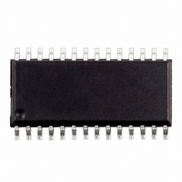
M41T94MH6F STMicroelectronics, M41T94MH6F Datasheet - Page 11

M41T94MH6F
Manufacturer Part Number
M41T94MH6F
Description
IC RTC SPI SRAM SER 64X8 28-SOIC
Manufacturer
STMicroelectronics
Type
Clock/Calendar/Alarmr
Datasheet
1.M41T94MH6F.pdf
(41 pages)
Specifications of M41T94MH6F
Memory Size
44B
Time Format
HH:MM:SS:hh (24 hr)
Date Format
YY-MM-DD-dd
Interface
SPI, 3-Wire Serial
Voltage - Supply
2.7 V ~ 5.5 V
Operating Temperature
-40°C ~ 85°C
Mounting Type
Surface Mount
Package / Case
28-SOIC, 28-SOH (8.48mm Width)
Bus Type
Serial (SPI)
User Ram
64Byte
Operating Supply Voltage (typ)
3.3/5V
Package Type
SOH
Operating Supply Voltage (max)
5.5V
Operating Supply Voltage (min)
2.7V
Operating Temperature Classification
Industrial
Operating Temperature (max)
85C
Operating Temperature (min)
-40C
Pin Count
28
Mounting
Surface Mount
Lead Free Status / RoHS Status
Lead free / RoHS Compliant
Other names
497-5372-2
M41T94MH6F
M41T94MH6F
Available stocks
Company
Part Number
Manufacturer
Quantity
Price
Company:
Part Number:
M41T94MH6F
Manufacturer:
AOS
Quantity:
26 700
Part Number:
M41T94MH6F
Manufacturer:
ST
Quantity:
20 000
M41T94
2
2.1
2.2
2.3
2.4
Signal description
Serial data output (SDO)
The output pin is used to transfer data serially out of the memory. Data is shifted out on the
falling edge of the serial clock.
Serial data input (SDI)
The input pin is used to transfer data serially into the device. Instructions, addresses, and
the data to be written, are each received this way. Input is latched on the rising edge of the
serial clock.
Serial clock (SCL)
The serial clock provides the timing for the serial interface (as shown in
and
on the rising edge of the clock input. The output data on the SDO pin changes state after the
falling edge of the clock input.
The M41T94 can be driven by a microcontroller with its SPI peripheral running in either of
the two following modes:
●
●
For these two modes, input data (SDI) is latched in by the low-to-high transition of clock
SCL, and output data (SDO) is shifted out on the high-to-low transition of SCL (see
on page 10
Chip enable (E)
When E is high, the memory device is deselected, and the SDO output pin is held in its high
impedance state. After power-on, a high-to-low transition on E is required prior to the start of
any operation.
Figure 8 on page
(CPOL, CPHA) = ('0', '0') or
(CPOL, CPHA) = ('1', '1').
and
Figure 6 on page
14). The W/R bit, addresses, or data are latched, from the input pin,
10).
Figure 7 on page 13
Signal description
Table 2
11/41


