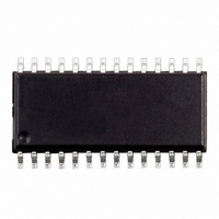
M41T94MH6F STMicroelectronics, M41T94MH6F Datasheet - Page 13

M41T94MH6F
Manufacturer Part Number
M41T94MH6F
Description
IC RTC SPI SRAM SER 64X8 28-SOIC
Manufacturer
STMicroelectronics
Type
Clock/Calendar/Alarmr
Datasheet
1.M41T94MH6F.pdf
(41 pages)
Specifications of M41T94MH6F
Memory Size
44B
Time Format
HH:MM:SS:hh (24 hr)
Date Format
YY-MM-DD-dd
Interface
SPI, 3-Wire Serial
Voltage - Supply
2.7 V ~ 5.5 V
Operating Temperature
-40°C ~ 85°C
Mounting Type
Surface Mount
Package / Case
28-SOIC, 28-SOH (8.48mm Width)
Bus Type
Serial (SPI)
User Ram
64Byte
Operating Supply Voltage (typ)
3.3/5V
Package Type
SOH
Operating Supply Voltage (max)
5.5V
Operating Supply Voltage (min)
2.7V
Operating Temperature Classification
Industrial
Operating Temperature (max)
85C
Operating Temperature (min)
-40C
Pin Count
28
Mounting
Surface Mount
Lead Free Status / RoHS Status
Lead free / RoHS Compliant
Other names
497-5372-2
M41T94MH6F
M41T94MH6F
Available stocks
Company
Part Number
Manufacturer
Quantity
Price
Company:
Part Number:
M41T94MH6F
Manufacturer:
AOS
Quantity:
26 700
Part Number:
M41T94MH6F
Manufacturer:
ST
Quantity:
20 000
M41T94
3.1
Figure 7.
E
SCL
SDI
SDO
SPI bus characteristics
The serial peripheral interface (SPI) bus is intended for synchronous communication
between different ICs. It consists of four signal lines: serial data input (SDI), serial data
output (SDO), serial clock (SCL) and a chip enable (E).
By definition a device that gives out a message is called “transmitter,” the receiving device
that gets the message is called “receiver.” The device that controls the message is called
“master.” The devices that are controlled by the master are called “slaves.”
The E input is used to initiate and terminate a data transfer. The SCL input is used to
synchronize data transfer between the master (micro) and the slave (M41T94) devices.
The SCL input, which is generated by the microcontroller, is active only during address and
data transfer to any device on the SPI bus (see
The M41T94 can be driven by a microcontroller with its SPI peripheral running in either of
the two following modes:
●
●
For these two modes, input data (SDI) is latched in by the low-to-high transition of clock
SCL, and output data (SDO) is shifted out on the high-to-low transition of SCL (see
on page 10
There is one clock for each bit transferred. Address and data bits are transferred in groups
of eight bits. Due to memory size the second most significant address bit is a Don’t Care
(address bit 6).
Input timing requirements
(CPOL, CPHA) = ('0', '0') or
(CPOL, CPHA) = ('1', '1').
tDVCH
and
Figure 6 on page
MSB IN
HIGH IMPEDANCE
tELCH
tCHDX
10).
tDLDH
tDHDL
tCLCH
Figure 5 on page
tCHEH
LSB IN
tCHCL
tEHEL
9).
tEHCH
Operation
AI04633
Table 2
13/41


