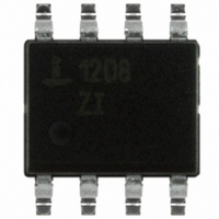
ISL1208IB8Z-TK Intersil, ISL1208IB8Z-TK Datasheet - Page 10

ISL1208IB8Z-TK
Manufacturer Part Number
ISL1208IB8Z-TK
Description
IC RTC LP BATT BACKED SRAM 8SOIC
Manufacturer
Intersil
Type
Clock/Calendar/NVSRAMr
Datasheet
1.ISL1208IB8Z-TK.pdf
(24 pages)
Specifications of ISL1208IB8Z-TK
Memory Size
2B
Time Format
HH:MM:SS (12/24 hr)
Date Format
YY-MM-DD-dd
Interface
I²C, 2-Wire Serial
Voltage - Supply
2.7 V ~ 5.5 V
Operating Temperature
-40°C ~ 85°C
Mounting Type
Surface Mount
Package / Case
8-SOIC (3.9mm Width)
Lead Free Status / RoHS Status
Lead free / RoHS Compliant
Other names
ISL1208IB8Z-TKTR
Available stocks
Company
Part Number
Manufacturer
Quantity
Price
Company:
Part Number:
ISL1208IB8Z-TK
Manufacturer:
STC
Quantity:
1 000
Part Number:
ISL1208IB8Z-TK
Manufacturer:
INTERSIL
Quantity:
20 000
Accuracy of the Real Time Clock
The accuracy of the Real Time Clock depends on the
frequency of the quartz crystal that is used as the time base
for the RTC. Since the resonant frequency of a crystal is
temperature dependent, the RTC performance will also be
dependent upon temperature. The frequency deviation of
the crystal is a function of the turnover temperature of the
crystal from the crystal’s nominal frequency. For example, a
~20ppm frequency deviation translates into an accuracy of
~1 minute per month. These parameters are available from
the crystal manufacturer. The ISL1208 provides on-chip
crystal compensation networks to adjust load capacitance to
tune oscillator frequency from -94ppm to +140ppm. For
more detailed information. See “Application Section” on
page 18.
Single Event and Interrupt
The alarm mode is enabled via the ALME bit. Choosing
single event or interrupt alarm mode is selected via the IM
bit. Note that when the frequency output function is enabled,
the alarm function is disabled.
The standard alarm allows for alarms of time, date, day of
the week, month, and year. When a time alarm occurs in
single event mode, an IRQ pin will be pulled low and the
alarm status bit (ALM) will be set to “1”.
The pulsed interrupt mode allows for repetitive or recurring
alarm functionality. Hence, once the alarm is set, the device
will continue to alarm for each occurring match of the alarm
and present time. Thus, it will alarm as often as every minute
(if only the nth second is set) or as infrequently as once a
year (if at least the nth month is set). During pulsed interrupt
mode, the IRQ pin will be pulled low for 250ms and the alarm
status bit (ALM) will be set to “1”.
NOTE: The ALM bit can be reset by the user or cleared
automatically using the auto reset mode (see ARST bit).
The alarm function can be enabled/disabled during battery
backup mode using the FOBATB bit. For more information
on the alarm, See “Alarm Registers” on page 14.
Frequency Output Mode
The ISL1208 has the option to provide a frequency output
signal using the IRQ/FOUT pin. The frequency output mode
is set by using the FO bits to select 15 possible output
frequency values from 0kHz to 32kHz. The frequency output
can be enabled/disabled during battery backup mode using
the FOBATB bit.
General Purpose User SRAM
The ISL1208 provides 2 bytes of user SRAM. The SRAM will
continue to operate in battery backup mode. However, it
should be noted that the I
backup mode.
2
C bus is disabled in battery
10
ISL1208
I
The ISL1208 has an I
access to the control and status registers and the user
SRAM. The I
industry I
signal (SDA) and a clock signal (SCL).
Oscillator Compensation
The ISL1208 provides the option of timing correction due to
temperature variation of the crystal oscillator for either
manufacturing calibration or active calibration. The total
possible compensation is typically -94ppm to +140ppm. Two
compensation mechanisms that are available are as follows:
Also provided is the ability to adjust the crystal capacitance
when the ISL1208 switches from V
mode. See “Battery Backup Mode (V
(V
Register Descriptions
The battery-backed registers are accessible following a
slave byte of “1101111x” and reads or writes to addresses
[00h:13h]. The defined addresses and default values are
described in Table 1. Address 09h is not used. Reads or
writes to 09h will not affect operation of the device but should
be avoided.
REGISTER ACCESS
The contents of the registers can be modified by performing
a byte or a page write operation directly to any register
address.
The registers are divided into 4 sections. These are:
There are no addresses above 13h.
2
1. An analog trimming (ATR) register that can be used to
2. A digital trimming register (DTR) that can be used to
1. Real Time Clock (7 bytes): Address 00h to 06h.
2. Control and Status (5 bytes): Address 07h to 0Bh.
3. Alarm (6 bytes): Address 0Ch to 11h.
4. User SRAM (2 bytes): Address 12h to 13h.
C Serial Interface
DD
adjust individual on-chip digital capacitors for oscillator
capacitance trimming. The individual digital capacitor is
selectable from a range of 9pF to 40.5pF (based upon
32.758kHz). This translates to a calculated
compensation of approximately -34ppm to +80ppm. (See
ATR description on page 18).
adjust the timing counter by ±60ppm. (See DTR
description on page 18).
)” on page 9.
2
C serial bus protocols using a bidirectional data
2
C serial interface is compatible with other
2
C serial bus interface that provides
DD
BAT
to battery backup
) to Normal Mode
September 12, 2008
FN8085.8


