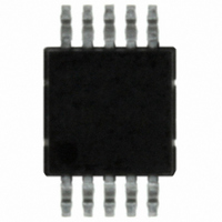
ISL1220IUZ-T Intersil, ISL1220IUZ-T Datasheet - Page 10

ISL1220IUZ-T
Manufacturer Part Number
ISL1220IUZ-T
Description
IC RTC LP BATT BACK SRAM 10MSOP
Manufacturer
Intersil
Type
Clock/Calendar/Alarmr
Datasheet
1.ISL1220IUZ-T.pdf
(20 pages)
Specifications of ISL1220IUZ-T
Memory Size
8B
Time Format
HH:MM:SS (12/24 hr)
Date Format
YY-MM-DD-dd
Interface
I²C, 2-Wire Serial
Voltage - Supply
2.7 V ~ 5.5 V
Operating Temperature
-40°C ~ 85°C
Mounting Type
Surface Mount
Package / Case
10-MSOP, Micro10™, 10-uMAX, 10-uSOP
Lead Free Status / RoHS Status
Lead free / RoHS Compliant
Other names
ISL1220IUZ-TTR
Available stocks
Company
Part Number
Manufacturer
Quantity
Price
Company:
Part Number:
ISL1220IUZ-T
Manufacturer:
Vishay
Quantity:
1 600
Write capability is allowable into the RTC registers (00h to
06h) only when the WRTC bit (bit 4 of address 07h) is set to
“1”. A multi-byte read or write operation is limited to one
section per operation. Access to another section requires a
new operation. A read or write can begin at any address
within the section.
A register can be read by performing a random read at any
address at any time. This returns the contents of that register
location. Additional registers are read by performing a
sequential read. For the RTC and Alarm registers, the read
ADDR. SECTION
0Ch
0Dh
0Ah
0Bh
0Eh
0Fh
00h
01h
02h
03h
04h
05h
06h
07h
08h
09h
10h
11h
12h
13h
14h
15h
16h
17h
18h
19h
Control
Status
Alarm
User
RTC
and
NAME
USR1
USR2
USR3
USR4
USR5
USR6
USR7
USR8
MNA
MOA
DWA
REG
DTR
SCA
HRA
ATR
DTA
MO
DW
INT
MN
HR
SC
DT
YR
SR
Reserved
BMATR1
USR17
USR27
USR37
USR47
USR57
USR67
USR77
USR87
EMNA
EMOA
EDWA
10
ESCA
EHRA
ARST
EDTA
YR23
MIL
IM
0
0
0
0
0
7
XTOSCB Reserved
BMATR0
AMN22
ASC22
USR16
USR26
USR36
USR46
USR56
USR66
USR76
USR86
MN22
ALME
SC22
YR22
6
0
0
0
0
0
0
0
0
TABLE 1. REGISTER MEMORY MAP
LPMODE FOBATB
AMN21
ASC21
AHR21
ADT21
USR15
USR25
USR35
USR45
USR55
USR65
USR75
USR85
MN21
SC21
HR21
YR21
DT21
ATR5
5
0
0
0
0
AMO20
AMN20
AHR20
USR14
USR24
USR34
USR44
USR54
USR64
USR74
USR84
ISL1220
ASC20
ADT20
WRTC
Reserved
MN20
MO20
SC20
HR20
YR20
ATR4
DT20
4
0
0
BIT
Reserved
AMO13
instruction latches all clock registers into a buffer, so an
update of the clock does not change the time being read. A
sequential read will not result in the output of data from the
memory array. At the end of a read, the master supplies a
stop condition to end the operation and free the bus. After a
read, the address remains at the previous address +1 so the
user can execute a current address read and continue
reading the next register.
It is not necessary to set the WRTC bit prior to writing into
the control and status, alarm, and user SRAM registers.
AMN13
AHR13
USR13
USR23
USR33
USR43
USR53
USR63
USR73
USR83
ASC13
ADT13
MN13
MO13
SC13
HR13
YR13
ATR3
DT13
FO3
3
0
0
AMN12
AMO12
ADW12
AHR12
USR12
USR22
USR32
USR42
USR52
USR62
USR72
USR82
ASC12
ADT12
MN12
MO12
DTR2
SC12
HR12
DT12
YR12
ATR2
DW2
ALM
FO2
2
AMO11
ADW11
AMN11
USR11
USR21
USR31
USR41
USR51
USR61
USR71
USR81
ASC11
AHR11
ADT11
MN11
MO11
DTR1
SC11
HR11
YR11
ATR1
DT11
DW1
BAT
FO1
1
ADW10
AMN10
AMO10
ASC10
AHR10
USR10
USR20
USR30
USR40
USR50
USR60
USR70
USR80
ADT10
MO10
MN10
HR10
RTCF
DTR0
SC10
DT10
YR10
ATR0
DW0
FO0
0
RANGE
00-59
00-59
0-59
0-59
0-23
1-31
1-12
0-99
0-23
1-31
1-12
N/A
N/A
N/A
N/A
N/A
N/A
N/A
N/A
N/A
N/A
N/A
N/A
N/A
0-6
0-6
June 22, 2006
DEFAULT
00h
00h
00h
00h
00h
00h
00h
01h
00h
00h
00h
00h
00h
00h
00h
00h
00h
00h
00h
00h
00h
00h
00h
00h
00h
00h
FN6315.0


