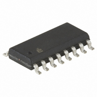
CDP68HC68T1M2 Intersil, CDP68HC68T1M2 Datasheet - Page 11

CDP68HC68T1M2
Manufacturer Part Number
CDP68HC68T1M2
Description
IC RTC 32X8 NVSRAM CMOS 16-SOIC
Manufacturer
Intersil
Type
Clock/Calendar/NVSRAMr
Datasheet
1.CDP68HC68T1EZ.pdf
(23 pages)
Specifications of CDP68HC68T1M2
Memory Size
32B
Time Format
HH:MM:SS (12/24 hr)
Date Format
YY-MM-DD-dd
Interface
SPI, 3-Wire Serial
Voltage - Supply
3 V ~ 6 V
Operating Temperature
-40°C ~ 85°C
Mounting Type
Surface Mount
Package / Case
16-SOIC (0.300", 7.5mm Width)
Digital Ic Case Style
SOIC
No. Of Pins
16
Operating Temperature Range
-40°C To +85°C
Peak Reflow Compatible (260 C)
No
Current Rating
12A
Leaded Process Compatible
No
Rohs Compliant
No
Bus Type
Serial (3-Wire, SPI)
Operating Supply Voltage (typ)
3.3/5V
Package Type
SOIC W
Operating Supply Voltage (max)
6V
Operating Supply Voltage (min)
3V
Operating Temperature Classification
Industrial
Operating Temperature (max)
85C
Operating Temperature (min)
-40C
Pin Count
16
Mounting
Surface Mount
Lead Free Status / RoHS Status
Contains lead / RoHS non-compliant
Available stocks
Company
Part Number
Manufacturer
Quantity
Price
Company:
Part Number:
CDP68HC68T1M2Z
Manufacturer:
Intersil
Quantity:
1 716
Part Number:
CDP68HC68T1M2Z
Manufacturer:
INTERSIL
Quantity:
20 000
NOTES:
V
This input is connected to the system voltage. After the CPU
initiates power down by setting Bit 6 in the Interrupt Control
Register to “1”, the level on this pin will terminate power
down if it rises about 1.0V above the level at the V
pin after previously falling below V
power-down is terminated, the PSE pin will return high and
the Clock Output will be enabled. The CPUR output pin will
also return high. The logic level present at this pin at the end
of POR determines the CDP68HC68T1’s operating mode.
V
The oscillator power source. The positive terminal of the
battery should be connected to this pin. When the level on
the V
internally connected to the V
V
the connection from V
the “LINE” input is used as the frequency source, V
may be tied to V
V
“XTAL IN” pin can be tied to V
XTAL IN, XTAL OUT
These pins are connected to a 32,768Hz. 1.048576MHz,
2.097152MHz or 4.194304MHz crystal. If an external clock
is used, it should be connected to “XTAL IN” with ‘XTAL
OUT” left open.
V
The positive power-supply pin.
Clock Control Register
Start-Stop
A high written into this bit will enable the counter stages of
the clock circuitry. A low will hold all bits reset in the divider
chain from 32Hz to 1Hz. A clock out selected by Bit 0, Bit 1
and Bit 2 will not be affected by the stop function except the
1Hz and 2Hz outputs.
7. All frequencies recommended oscillator circuit. C
8. R is used for 32KHz operation only. 100k to 300k range as
SYS
SS
SYS
BATT
DD
crystal dependent.
specified by crystal manufacturer.
if V
SYS
rises a threshold above (1.0V) the voltage on V
BATT
pin falls below V
is at V
FIGURE 7. OSCILLATOR CIRCUIT
T1
DD
XTAL
XTAL
OUT
IN
or V
SS
BATT
. If V
22M
SS
BATT
. The “XTAL IN” pin must be at
BATT
to the V
DD
11
SS
C2
+1.0V, the V
pin. When the voltage on
is connected to V
or V
BATT
DD
DD
5pF TO 30pF
10pF TO 40pF
pin is opened. When
+1.0V. When
.
C1
BATT
1
, C
BATT
pin will be
2
DD
BATT
values
BATT
, the
CDP68HC68T1
input
,
Line-XTAL
When this bit is set high, clock operation will use the
50-cycle or 60-cycle input present at the LINE input pin.
When the bit is low, the crystal input will generate the 1Hz
time update.
XTAL Select
One of 4 possible crystals is selected by value in these two
bits:
50Hz to 60Hz
50Hz is selected as the line input frequency when this bit is
set high. A low will select 60Hz. The power-sense bit in the
Interrupt Control Register must be set low for line frequency
operation.
Clock Out
The three bits specify one of the 7 frequencies to be used as
the squarewave clock output:
All bits are reset by a power-on reset. Therefore, the XTAL is
selected as the clock output at this time.
Interrupt Control Register
Watchdog
When this bit is set high, the watchdog operation will be
enabled. This function requires the CPU to toggle the CE pin
periodically without a serial-transfer requirement. In the
event this does not occur, a CPU reset will be issued. Status
Register must be read before re-enabling watchdog.
Power-Down
A high in this location will initiate a power down. A CPU reset
will occur, the CLK OUT and PSE output pins will be set low
and the serial interface will be disabled.
Power Sense
This bit is used to enable the line input pin to sense a power
failure. It is set high for this function. When power sense is
selected, the input to the 50Hz to 60Hz prescaler is
disconnected. Therefore, crystal operation is required when
power sense is enabled. An interrupt is generated when a
power failure is sensed and the power sense and Interrupt
True bit in the Status Register are set. When power sense is
activated, a “0” must be written to this location followed by a
“1” to re-enable power sense.
0 = 4.194304MHz
1 = 2.097152MHz
0 = XTAL
1 = XTAL/2
2 = XTAL/4
3 = XTAL/8
3 = 32,768Hz
4 = Disable (low output)
2 = 1.048576MHz
5 = 1Hz
6 = 2Hz
7 = 50Hz or 60Hz
XTAL Operation = 64Hz
October 29, 2007
FN1547.8


