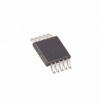
DS1374U-3+ Maxim Integrated Products, DS1374U-3+ Datasheet - Page 2

DS1374U-3+
Manufacturer Part Number
DS1374U-3+
Description
IC RTC I2C W/CHARGER 10-USOP
Manufacturer
Maxim Integrated Products
Type
Watchdog Timer/Trickle Chargerr
Datasheet
1.DS1374U-33.pdf
(18 pages)
Specifications of DS1374U-3+
Time Format
Binary
Date Format
Binary
Interface
I²C, 2-Wire Serial
Voltage - Supply
2.7 V ~ 3.3 V
Operating Temperature
-40°C ~ 85°C
Mounting Type
Surface Mount
Package / Case
10-MSOP, Micro10™, 10-uMAX, 10-uSOP
Lead Free Status / RoHS Status
Lead free / RoHS Compliant
Memory Size
-
ABSOLUTE MAXIMUM RATINGS
Voltage Range on V
Voltage Range on SDA or SCL
Junction-to-Ambient Thermal Resistance (θ
I
Trickle Charger and Reset Input/Output
RECOMMENDED DC OPERATING CONDITIONS
(V
Note 1: Package thermal resistances were obtained using the method described in JEDEC specification JESD51-7, using a four-
Stresses beyond those listed under “Absolute Maximum Ratings” may cause permanent damage to the device. These are stress ratings only, and functional
operation of the device at these or any other conditions beyond those indicated in the operational sections of the specifications is not implied. Exposure to
absolute maximum rating conditions for extended periods may affect device reliability.
2
Supply Voltage
(Notes 3, 4)
Input Logic 1
Input Logic 0
Pullup Resistor Voltage (INT,
SQW, SDA, SCL), V
Power-Fail Voltage
(Note 3)
Backup Supply Voltage
(Notes 3, 4, 5)
2
CC
Relative to Ground ....................................-0.3V to V
16-Pin SO .....................................................................73°C/W
10-Pin µSOP ...............................................................221°C/W
C, 32-Bit Binary Counter Watchdog RTC with
_____________________________________________________________________
= V
CC(MIN)
layer board. For detailed information on package thermal considerations, refer to www.maxim-ic.com/thermal-tutorial.
PARAMETER
to V
CC
CC
CC(MAX)
Pin Relative to Ground .....-0.3V to +6.0V
= 0V
, T
A
= -40°C to +85°C, unless otherwise noted.) (Note 2)
SYMBOL
V
BACKUP
V
V
V
V
V
CC
PU
PF
IH
IL
JA
) (Note 1)
DS1374-33
DS1374-3
DS1374-18
(Note 3)
(Note 3)
(Note 3)
DS1374-33
DS1374-3
DS1374-18
DS1374-33
DS1374-3, DS1374-18
CC
+ 0.3V
CONDITIONS
Junction-to-Case Thermal Resistance (θ
Operating Temperature Range ...........................-40°C to +85°C
Storage Temperature Range .............................-55°C to +125°C
Lead Temperature (soldering, 10s) .................................+260°C
Soldering Temperature (reflow) .......................................+260°C
16-Pin SO .....................................................................23°C/W
10-Pin µSOP .................................................................39°C/W
0.7 x V
2.97
1.71
2.70
2.45
1.51
MIN
-0.3
2.7
1.3
1.3
CC
TYP
2.88
3.3
3.0
1.8
2.6
1.6
3.0
3.0
JC
) (Note 1)
V
CC
+0.3 x
(
MAX
5.50
1.89
2.97
1.71
V
V
MAX)
3.3
+ 0.3
5.5
2.7
3.7
CC
CC
UNITS
V
V
V
V
V
V


