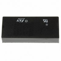
M48T512Y-70PM1 STMicroelectronics, M48T512Y-70PM1 Datasheet - Page 2

M48T512Y-70PM1
Manufacturer Part Number
M48T512Y-70PM1
Description
IC TIMEKPR NVRAM 4MBIT 5V 32-DIP
Manufacturer
STMicroelectronics
Series
Timekeeper®r
Type
Clock/Calendar/NVSRAMr
Specifications of M48T512Y-70PM1
Memory Size
4M (512K x 8)
Time Format
HH:MM:SS (24 hr)
Date Format
YY-MM-DD-dd
Interface
Parallel
Voltage - Supply
4.5 V ~ 5.5 V
Operating Temperature
0°C ~ 70°C
Mounting Type
Through Hole
Package / Case
32-DIP (600 mil) Module
Clock Format
BCD
Clock Ic Type
Timekeeper
Memory Configuration
512K X 8
Supply Voltage Range
4.5V To 5.5V
Digital Ic Case Style
DIP
No. Of Pins
32
Operating Temperature Range
0°C To +70°C
Rohs Compliant
Yes
Nvram Features
RTC, Internal Battery, XTAL
Access Time
70ns
Memory Case Style
DIP
Bus Type
Parallel
User Ram
512KB
Operating Supply Voltage (typ)
5V
Operating Supply Voltage (max)
5.5V
Operating Supply Voltage (min)
4.5V
Operating Temperature Classification
Commercial
Operating Temperature (max)
70C
Operating Temperature (min)
0C
Pin Count
32
Mounting
Through Hole
Lead Free Status / RoHS Status
Contains lead / RoHS non-compliant
Other names
497-2856-5
Available stocks
Company
Part Number
Manufacturer
Quantity
Price
Company:
Part Number:
M48T512Y-70PM1
Manufacturer:
NIPPON
Quantity:
34 000
M48T512Y, M48T512V
Table 2. Absolute Maximum Ratings
Note: 1. Stresses greater than those listed under "Absolute Maximum Ratings" may cause permanent damage to the device. This is a stress
Figure 2. DIP Connections
The M48T512Y/V directly replaces industry stan-
dard 512Kb x 8 SRAMs. It also provides the non-
volatility of Flash without any requirement for spe-
cial write timing or limitations on the number of
writes that can be performed.
2/14
Symbol
T
T
SLD
V
CAUTION: Negative undershoots below –0.3V are not allowed on any pin while in the Battery Back-up mode.
2. Soldering temperature not to exceed 260°C for 10 seconds (total thermal budget not to exceed 150°C for longer than 30 seconds).
V
P
T
STG
I
CC
O
IO
A
D
rating only and functional operation of the device at these or any other conditions above those indicated in the operational section
of this specification is not implied. Exposure to the absolute maximum rating conditions for extended periods of time may affect
reliability.
(2)
DQ0
DQ1
DQ2
V SS
A18
A16
A14
A12
A7
A6
A5
A4
A3
A2
A1
A0
Ambient Operating Temperature
Storage Temperature (V
Lead Solder Temperature for 10 seconds
Input or Output Voltages
Supply Voltage
Output Current
Power Dissipation
1
2
3
4
5
6
7
8
9
10
11
12
13
14
15
16
M48T512Y
M48T512V
AI02263
32
31
30
29
28
27
26
25
24
23
22
21
20
19
18
17
CC
V CC
A15
A17
W
A13
A8
A9
A11
G
A10
E
DQ7
DQ6
DQ5
DQ4
DQ3
Off, Oscillator Off)
Parameter
(1)
The 32 pin 600 mil DIP Hybrid houses a controller
chip, SRAM, quartz crystal, and a long life lithium
button cell in a single package. Figure 3 illustrates
the static memory array and the quartz controlled
clock oscillator. The clock locations contain the
year, month, date, day, hour, minute, and second
in 24 hour BCD format. Corrections for 28, 29
(leap year - compliant until the year 2100), 30, and
31 day months are made automatically. Byte
7FFF8h is the clock control register. This byte con-
trols user access to the clock information and also
stores the clock calibration setting. The seven
clock bytes (7FFFFh-7FFF9h) are not the actual
clock counters, they are memory locations consist-
ing of BiPORT™ read/write memory cells within
the static RAM array. The M48T512Y/V includes a
clock control circuit which updates the clock bytes
with current information once per second. The in-
formation can be accessed by the user in the
same manner as any other location in the static
memory array. The M48T512Y/V also has its own
Power-Fail Detect circuit. This control circuitry
constantly monitors the supply voltage for an out
of tolerance condition. When V
ance, the circuit write protects the TIMEKEEPER
register data and external SRAM, providing data
security in the midst of unpredictable system oper-
ation. As V
cally switches to the battery, maintaining data and
clock operation until valid power is restored.
READ MODE
The M48T512Y/V is in the Read Mode whenever
W (Write Enable) is high and E (Chip Enable) is
low. The unique address specified by the 19 Ad-
dress Inputs defines which one of the 524,288
bytes of data is to be accessed. Valid data will be
available at the Data I/O pins within Address Ac-
M48T512Y
M48T512V
CC
falls, the control circuitry automati-
–0.3 to V
–0.3 to 7.0
–0.3 to 4.6
–40 to 85
0 to 70
Value
260
20
1
CC
CC
+0.3
is out of toler-
Unit
mA
°C
°C
°C
W
V
V
V


