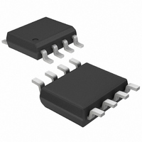
DS1388Z-3+T&R Maxim Integrated Products, DS1388Z-3+T&R Datasheet - Page 14

DS1388Z-3+T&R
Manufacturer Part Number
DS1388Z-3+T&R
Description
IC RTC I2C W/CHARGER 8-SOIC
Manufacturer
Maxim Integrated Products
Type
Clock/Calendar/Supervisor/EEPROMr
Datasheet
1.DS1388Z-33.pdf
(19 pages)
Specifications of DS1388Z-3+T&R
Memory Size
4K (512 x 8)
Time Format
HH:MM:SS:hh (12/24 hr)
Date Format
YY-MM-DD-dd
Interface
I²C, 2-Wire Serial
Voltage - Supply
2.7 V ~ 3.3 V
Operating Temperature
-40°C ~ 85°C
Mounting Type
Surface Mount
Package / Case
8-SOIC (3.9mm Width)
Lead Free Status / RoHS Status
Lead free / RoHS Compliant
I
and 512 Bytes EEPROM
The DS1388 provides 512 bytes of EEPROM organized
into two blocks of 256 bytes. Each 256-byte block is
divided into 32 pages consisting of 8 bytes per page.
The EEPROM can be written one page at a time. Page
write operations are limited to writing bytes within a sin-
gle physical page, regardless of the number of bytes
actually being written. Physical page boundaries start at
addresses that are integer multiples of the page size (8
bytes) and end at addresses that are integer multiples
of [page size -1]. For example, page 0 contains word
addresses 00h to 07h. Similarly, page 1 contains word
addresses 08h to 0Fh. If a page write command
attempts to write across a physical page boundary, the
result is that the data wraps around to the beginning of
the current page (overwriting data previously stored
there), instead of being written to the next page as
might be expected. Therefore, it is necessary for the
application software to prevent page write operations
that would attempt to cross a page boundary.
The DS1388 supports a bidirectional I
transmission protocol. A device that sends data onto
the bus is defined as a transmitter and a device receiv-
ing data is defined as a receiver. The device that con-
trols the message is called a master. The devices that
are controlled by the master are slaves. The bus must
be controlled by a master device that generates the
serial clock (SCL), controls the bus access, and gener-
ates the START and STOP conditions. The DS1388
Figure 5. Programmable Trickle Charger
14
2
C RTC/Supervisor with Trickle Charger
____________________________________________________________________
V
TRICKLE-CHARGE REGISTER (00Ah)
CC
TCS3
BIT 7
NOTE: ONLY 1010b ENABLES CHARGER
TCS2
BIT 6
1 0F 16 SELECT
TCS1
BIT 5
I
2
C Serial Data Bus
TCS0
BIT 4
2
BIT 3
DS1
C bus and data
EEPROM
SELECT
1 OF 2
BIT 2
DS0
ROUT1
BIT 1
SELECT
1 OF 3
ROUT0
operates as a slave on the I
bus are made through the open-drain I/O lines SDA
and SCL. Within the bus specifications, a standard
mode (100kHz maximum clock rate) and a fast mode
(400kHz maximum clock rate) are defined. The DS1388
works in both modes.
The following bus protocol has been defined (Figure 6):
• Data transfer can be initiated only when the bus is
• During data transfer, the data line must remain stable
Accordingly, the following bus conditions have been
defined:
BIT 0
Bus not busy: Both data and clock lines remain
high.
Start data transfer: A change in the state of the data
line from high to low, while the clock line is high,
defines a START condition.
Stop data transfer: A change in the state of the data
line from low to high, while the clock line is high,
defines a STOP condition.
Data valid: The state of the data line represents valid
data when, after a START condition, the data line is
stable for the duration of the high period of the clock
signal. The data on the line must be changed during
the low period of the clock signal. There is one clock
pulse per bit of data.
not busy.
whenever the clock line is high. Changes in the data
line while the clock line is high will be interpreted as
control signals.
TCS
DS
ROUT
0-1
0-3
0-1
= DIODE SELECT
= TRICKLE-CHARGE SELECT
= RESISTOR SELECT
2
250Ω
2kΩ
4kΩ
C bus. Connections to the
R1
R2
R3
V
BACKUP


