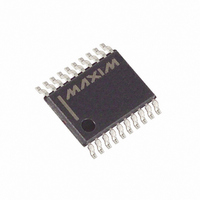
DS1677E Maxim Integrated Products, DS1677E Datasheet

DS1677E
Specifications of DS1677E
Available stocks
Related parts for DS1677E
DS1677E Summary of contents
Page 1
... VOLTAGE PIN- PART* (V) PACKAGE DS1677E 5.0 20 TSSOP DS1677E+ 5.0 20 TSSOP * All devices are specified over the 0°C to +70°C operating range. † A “‘+” anywhere on the top mark denotes a lead(Pb)-free device. + Denotes a lead(Pb)-free/RoHS-compliant device. Portable System Controller FEATURES ...
Page 2
DETAILED DESCRIPTION The microprocessor monitor circuitry of the DS1677 provides three basic functions. First, a precision temperature-compensated reference and comparator circuit monitors the status of V tolerance condition occurs, an internal power-fail signal is generated which forces the to state. ...
Page 3
PIN DESCRIPTION PIN NAME Battery Input for Standard 3V Lithium Cell or Other Energy Source. UL recognized ensure against reverse charging when used with a lithium battery BAT ic.com/qa/info/ul/. External SRAM Power Supply Output. This ...
Page 4
POWER-UP/POWER-DOWN CONSIDERATIONS When V is applied to the DS1677 and reaches a level greater than V CC device becomes fully accessible after t When V drops below V CC CCSW During power-up, when V returns to an in-tolerance condition, the ...
Page 5
DS1677 ADDRESS MAP Figure 3 BIT7 SECONDS MINUTES A YEAR SEC ALARM 08 M ...
Page 6
TIME OF DAY ALARM BITS Table 1 ALARM REGISTER MASK BITS (BIT 7) SECONDS MINUTES HOURS SPECIAL PURPOSE REGISTERS The DS1677 has two additional registers (control register and status register) ...
Page 7
STATUS REGISTER BIT 7 BIT 6 CU LOBAT CU (Conversion Update In Progress). When this bit is a one, an update to the ADC Register (register 0Eh) will occur within 488 μs. When this bit is a zero, an update ...
Page 8
MICROPROCESSOR MONITOR The DS1677 monitors three vital conditions for a microprocessor: power supply, software execution, and external override. First, a precision temperature-compensated reference and comparator circuit monitors the status of V When an out-of-tolerance condition occurs, an internal power-fail signal ...
Page 9
ANALOG-TO-DIGITAL CONVERTER The DS1677 provides a 3-channel 8-bit analog-to-digital converter. The A/D reference voltage (2.55V typical) is derived from an on-chip band-gap circuit. Three multiplexed analog inputs are provided through the AIN0, AIN1, and AIN2 pins. The ADC is monotonic ...
Page 10
CU BIT TIMING Figure 5 3-WIRE SERIAL INTERFACE Communication with the DS1677 is accomplished through a simple 3-wire interface consisting of the Chip Select (CS), Serial Clock (SCLK) and Input/Output (I/O) pins. All data transfers are initiated by driving the ...
Page 11
SINGLE BYTE DATA TRANSFER Figure 6 MULTIPLE BYTE BURST TRANSFER Figure ...
Page 12
POWER-FAIL COMPARATOR Figure ...
Page 13
ABSOLUTE MAXIMUM RATINGS Voltage Range on Any Pin Relative to Ground……………………………………………..-0.3V to +7.0V Operating Temperature Range………………………………………………………………..0C to +70C Storage Temperature Range………………………………………………………………-55C to +125C Soldering Temperature………………………………………….See IPC/JEDEC J-STD-020 Specification This is a stress rating only and functional operation of the device ...
Page 14
CAPACITANCE PARAMETER Input Capacitance I/O Capacitance Crystal Capacitance AC ELECTRICAL CHARACTERISTICS PARAMETER Data to Clock Setup CLK to Data Hold CLK to Data Delay CLK to Low Time CLK to High Time CLK Frequency CLK Rise and Fall CS to ...
Page 15
TIMING DIAGRAM: READ DATA Figure 9 TIMING DIAGRAM: WRITE DATA Figure 10 PUSHBUTTON RESET Figure ...
Page 16
POWER-UP Figure 12 POWER-DOWN Figure ...
Page 17
POWER-FAIL WARNING Figure 14 NOTES: 1. All voltages are referenced to ground specified with outputs open, CS set to a logic 1, SCLK = 500kHz, oscillator enabled, and ADC CCA enabled specified with CS, ...
Page 18
... Maxim/Dallas Semiconductor cannot assume responsibility for use of any circuitry other than circuitry entirely embodied in a Maxim/Dallas Semiconductor product. No circuit patent licenses are implied. Maxim/Dallas Semiconductor reserves the right to change the circuitry and specifications without notice at any time The Maxim logo is a registered trademark of Maxim Integrated Products, Inc. The Dallas logo is a registered trademark of Dallas Semiconductor Corporation. DOCUMENT NO. 21-0066 © ...


