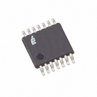
X1288V14I-4.5AT1 Intersil, X1288V14I-4.5AT1 Datasheet - Page 20

X1288V14I-4.5AT1
Manufacturer Part Number
X1288V14I-4.5AT1
Description
IC RTC/CAL/CPU SUP EE 14-TSSOP
Manufacturer
Intersil
Type
Clock/Calendar/Supervisor/EEPROMr
Datasheet
1.X1288S16.pdf
(27 pages)
Specifications of X1288V14I-4.5AT1
Memory Size
256K (32K x 8)
Time Format
HH:MM:SS:hh (12/24 hr)
Date Format
YY-MM-DD-dd
Interface
I²C, 2-Wire Serial
Voltage - Supply
4.5 V ~ 5.5 V
Operating Temperature
-40°C ~ 85°C
Mounting Type
Surface Mount
Package / Case
14-TSSOP
Lead Free Status / RoHS Status
Contains lead / RoHS non-compliant
ation, all inputs are disabled until completion of the
internal write cycle. Refer to Figure 14 for the address,
acknowledge, and data transfer sequence.
Stops and Write Modes
Stop conditions that terminate write operations must
be sent by the master after sending at least 1 full data
byte and it’s associated ACK signal. If a stop is issued
in the middle of a data byte, or before 1 full data byte +
ACK is sent, then the X1288 resets itself without per-
forming the write. The contents of the array are not
affected.
Acknowledge Polling
Disabling of the inputs during nonvolatile write cycles
can be used to take advantage of the typical 5mS write
cycle time. Once the stop condition is issued to indi-
cate the end of the master’s byte load operation, the
X1288 initiates the internal nonvolatile write cycle.
Acknowledge polling can begin immediately. To do
this, the master issues a start condition followed by the
Slave Address Byte for a write or read operation. If the
X1288 is still busy with the nonvolatile write cycle then
no ACK will be returned. When the X1288 has com-
Signals from
the Slave
Signals from
the Master
SDA Bus
S
a
r
t
t
20
1
Address
Slave
Signals from
the Master
SDA Bus
Signals from
the Slave
1
1
FIGURE 15. CURRENT ADDRESS READ SEQUENCE
1
0
A
C
K
FIGURE 14. PAGE WRITE SEQUENCE
0
Address 1
Word
S
a
t
r
t
1
X1288
Address
Slave
A
C
K
1
1
Address 0
pleted the write operation, an ACK is returned and the
host can proceed with the read or write operation.
Refer to the flow chart in Figure 16.
Read Operations
There are three basic read operations: Current
Address Read, Random Read, and Sequential Read.
Current Address Read
Internally the X1288 contains an address counter that
maintains the address of the last word read incre-
mented by one. Therefore, if the last read was to
address n, the next read operation would access data
from address n+1. On power-up, the sixteen bit
address is initialized to 0h. In this way, a current
address read immediately after the power-on reset
can download the entire contents of memory starting
at the first location.Upon receipt of the Slave Address
Byte with the R/W bit set to one, the X1288 issues an
acknowledge, then transmits eight data bits. The mas-
ter terminates the read operation by not responding
with an acknowledge during the ninth clock and issu-
ing a stop condition. Refer to Figure 15 for the
address, acknowledge, and data transfer sequence.
1
Word
1
A
C
K
Data
A
C
K
1 ≤ n ≤ 128 for EEPROM array
1 ≤ n ≤ 8 for CCR
Data
(1)
S
o
p
t
Data
(n)
C
A
K
S
o
p
t
April 14, 2006
FN8102.3


