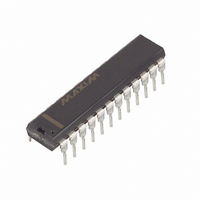
DS1742-70 Maxim Integrated Products, DS1742-70 Datasheet - Page 4

DS1742-70
Manufacturer Part Number
DS1742-70
Description
IC RTC RAM Y2K 5V 70NS 24-EDIP
Manufacturer
Maxim Integrated Products
Type
Clock/Calendar/NVSRAM/Y2Kr
Datasheet
1.DS1742-70.pdf
(15 pages)
Specifications of DS1742-70
Memory Size
16K (2K x 8)
Time Format
HH:MM:SS (24 hr)
Date Format
YY-MM-DD-dd
Interface
Parallel
Voltage - Supply
4.5 V ~ 5.5 V
Operating Temperature
0°C ~ 70°C
Mounting Type
Through Hole
Package / Case
24-DIP (600 mil) Module
Lead Free Status / RoHS Status
Contains lead / RoHS non-compliant
Available stocks
Company
Part Number
Manufacturer
Quantity
Price
Company:
Part Number:
DS1742-70IND
Manufacturer:
MAXIM
Quantity:
201
SETTING THE CLOCK
As shown in Table 2, bit 7 of the century register is the write bit. Setting the write bit to a 1, like the read
bit, halts updates to the DS1742 registers. The user can then load them with the correct day, date and time
data in 24-hour BCD format. Resetting the write bit to a 0 then transfers those values to the actual clock
counters and allows normal operation to resume.
STOPPING AND STARTING THE CLOCK OSCILLATOR
The clock oscillator may be stopped at any time. To increase the shelf life, the oscillator can be turned off
to minimize current drain from the battery. The
Table 2. Setting it to a 1 stops the oscillator.
FREQUENCY TEST BIT
As shown in Table 2, bit 6 of the day byte is the frequency test bit. When the frequency test bit is set to
logic 1 and the oscillator is running, the LSB of the seconds register will toggle at 512 Hz. When the
seconds register is being read, the DQ0 line will toggle at the 512 Hz frequency as long as conditions for
access remain valid (i.e.,
stable).
CLOCK ACCURACY
The DS1742 is guaranteed to keep time accuracy to within ±1 minute per month at 25°C. Dallas
Semiconductor calibrates the RTC at the factory using nonvolatile tuning elements. The DS1742 does not
require additional calibration. For this reason, methods of field clock calibration are not available and not
necessary. Clock accuracy is also affected by the electrical environment and caution should be taken to
place the RTC in the lowest level EMI section of the PCB layout. For additional information refer to
Application Note 58.
Table 2. REGISTER MAP
OSC = STOP BIT
W = WRITE BIT
Note: All indicated “X” bits are not used but must be set to “0” during write cycle to ensure proper clock operation.
ADDRESS
7FD
7FC
7FB
7FA
7FF
7FE
7F9
7F8
OSC
BF
B
W
X
X
X
X
7
R = READ BIT
X = SEE NOTE BELOW
FT
B
X
X
X
R
6
10 Year
CE
10 Minutes
10 Seconds
low,
B
X
X
10 Century
5
10 Hour
10 Date
OE
Month
low,
DATA
B
10
X
4
FT = FREQUENCY TEST
BF = BATTERY FLAG
WE
B
X
high, and address for seconds register remain valid and
OSC
4 of 15
3
bit is the MSB (bit 7) of the seconds registers, see
Minutes
Seconds
B
Century
Month
Hour
2
Year
Date
Day
B
1
B
0
FUNCTION
Minutes
Seconds
Control
Month
Hour
Year
Date
Day
RANGE
00–99
01–31
00–59
00–39
01–12
01–07
00–23
00–59


