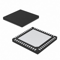
MAX19707ETM+ Maxim Integrated Products, MAX19707ETM+ Datasheet - Page 18

MAX19707ETM+
Manufacturer Part Number
MAX19707ETM+
Description
IC ANLG FRONT END 45MSPS 48-TQFN
Manufacturer
Maxim Integrated Products
Datasheet
1.MAX19707ETM.pdf
(37 pages)
Specifications of MAX19707ETM+
Number Of Bits
10
Number Of Channels
4
Power (watts)
84.6mW
Voltage - Supply, Analog
3V
Voltage - Supply, Digital
3V
Package / Case
48-TQFN Exposed Pad
Lead Free Status / RoHS Status
Lead free / RoHS Compliant
10-Bit, 45Msps, Ultra-Low-Power
Analog Front-End
18
Figure 3. Rx ADC System Timing Diagram
The dual, 10-bit digital-to-analog converter (Tx DAC)
operates with clock speeds up to 45MHz. The Tx DAC
digital inputs, D0–D9, are multiplexed on a single 10-bit
bus. The voltage reference determines the Tx DAC full-
scale output voltage. See the Reference Configurations
section for details on setting the reference voltage.
The Tx DAC outputs at IDN, IDP and QDN, QDP are
biased at a 0.7V to 1.05V adjustable DC common-
mode bias and designed to drive a differential input
stage with ≥ 70kΩ input impedance. This simplifies the
Table 2. Tx DAC Output Voltage vs. Input Codes
(Internal Reference Mode V
Full Scale)
DIFFERENTIAL OUTPUT VOLTAGE (V)
CHQ
D0–D9
CLK
CHI
t
______________________________________________________________________________________
DOQ
(
(
(
(
(
(
(
V
V
V
V
V
V
V
t
CL
FS
FS
FS
FS
FS
D0Q
FS
FS
)
)
)
)
)
)
)
t
V
−
−
V
V
−
CLK
V
REFDAC
REFDAC
V
V
REFDAC
REFDAC
V
1024
1024
1024
1024
REFDAC
REFDAC
REFDAC
1024
1024
1024
t
CH
D1I
×
×
×
×
×
×
×
1023
1023
REFDAC
1023
1023
1021
1023
t
DOI
1023
1023
1023
1023
1021
D1Q
3
1
1
Dual, 10-Bit Tx DAC
= 1.024V, External Reference Mode V
D2I
D2Q
5.5 CLOCK-CYCLE LATENCY (CHQ)
5 CLOCK-CYCLE LATENCY (CHI)
OFFSET BINARY (D0–D9)
D3I
11 1111 1111
11 1111 1110
10 0000 0001
10 0000 0000
01 1111 1111
00 0000 0001
00 0000 0000
D3Q
analog interface between RF quadrature upconverters
and the MAX19707. Many RF upconverters require a
0.7V to 1.05V common-mode bias. The Tx DAC DC
common-mode bias eliminates discrete level-setting
resistors and code-generated level shifting while pre-
serving the full dynamic range of each Tx DAC. The Tx
DAC differential analog outputs cannot be used in sin-
gle-ended mode because of the internally generated
common-mode DC level. Table 2 shows the Tx DAC
output voltage vs. input codes. Table 10 shows the
selection of DC common-mode levels. See Figure 4 for
an illustration of the Tx DAC analog output levels.
D4I
REFDAC
D4Q
= V
D5I
REFIN
INPUT DECIMAL CODE
; V
D5Q
FS
1023
1022
= ±400 for 800mV
513
512
511
1
0
D6I
D6Q
P-P


