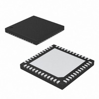
MAX19707ETM+ Maxim Integrated Products, MAX19707ETM+ Datasheet - Page 25

MAX19707ETM+
Manufacturer Part Number
MAX19707ETM+
Description
IC ANLG FRONT END 45MSPS 48-TQFN
Manufacturer
Maxim Integrated Products
Datasheet
1.MAX19707ETM.pdf
(37 pages)
Specifications of MAX19707ETM+
Number Of Bits
10
Number Of Channels
4
Power (watts)
84.6mW
Voltage - Supply, Analog
3V
Voltage - Supply, Digital
3V
Package / Case
48-TQFN Exposed Pad
Lead Free Status / RoHS Status
Lead free / RoHS Compliant
However, power consumption is higher in this mode
because both the Tx and Rx cores are always on. To
prevent bus contention in these states, the Rx ADC out-
put buffers are tri-stated during Tx and the Tx DAC
input bus is tri-stated during Rx.
In SLOW mode, the Rx ADC core is off during Tx; like-
wise the Tx DAC and filters are turned off during Rx to
yield lower power consumption in these modes. For
example, the power in SLOW Tx mode is 49.5mW. The
power consumption during Rx is 77.1mW compared to
84.6mW power consumption in FAST mode. However,
the recovery time between states is increased. The
switching time in SLOW mode between Rx to Tx is 7µs
and Tx to Rx is 4.1µs.
Bit E3 in the ENABLE-16 or ENABLE-8 register deter-
mines whether the device Tx-Rx mode is controlled
externally through the T/R input (E3 = low) or through the
SPI command (E3 = high). By default, the MAX19707 is
in the external Tx-Rx control mode. In the external control
Figure 6. Serial-Interface Timing Diagram
DOUT
SCLK
DIN
CS
t
CSW
DOUT = TRI-STATED WHEN
AUX-ADC IS IDLE
t
CSS
16-BIT OR 8-BIT WRITE INTO SPI (DIN)
D11 (16-BIT)
t
D3 (8-BIT)
DS
MSB
______________________________________________________________________________________
t
t
CH
External
DH
t
CP
t
D10 (16-BIT)
CL
D2 (8-BIT)
T/R R Switching Control vs.
Serial-Interface Control
DOUT = ACTIVE WHEN
BIT AD0 IS SET
LSB
A0
10-Bit, 45Msps, Ultra-Low-Power
t
CS
t
CSD
16-BIT OR 8-BIT WRITE
AUX-ADC CONVERSION
INTO SPI DURING
MSB
t
CONV
LSB
AUX-ADC
IS BUSY
mode, use the T/R input (pin 27) to switch between Rx
and Tx modes. Using the T/R pin provides faster switch-
ing between Rx and Tx modes. To override the external
Tx-Rx control, program the MAX19707 through the serial
interface. During SHDN, IDLE, or STBY modes, the T/R
input is overridden. To restore external Tx-Rx control,
program bit E3 low and exit the SHDN, IDLE, or STBY
modes through the serial interface.
The serial digital interface is a standard 3-wire connec-
tion compatible with SPI/QSPI™/MICROWIRE/DSP inter-
faces. Set CS low to enable the serial data loading at
DIN or output at DOUT. Following a CS high-to-low tran-
sition, data is shifted synchronously, most significant bit
first, on the rising edge of the serial clock (SCLK). After
16 bits are loaded into the serial input register, data is
transferred to the latch when CS transitions high. CS
must transition high for a minimum of 80ns before the
next write sequence. The SCLK can idle either high or
low between transitions. Figure 6 shows the detailed
timing diagram of the 3-wire serial interface.
QSPI is a trademark of Motorola, Inc.
t
DCS
DATA READY
AUX-ADC
BIT D11
SIMULTANEOUS 16-BIT WRITE INTO SPI (DIN)
10-BIT READ OUT OF AUX-ADC (DOUT) WITH
Analog Front-End
MSB
(DIN)
t
CD
BIT D10
(DOUT)
(DIN)
BIT D9
MSB
BIT D1
(DIN)
(DOUT)
BIT D0
LSB
BIT A0
(DIN)
LSB
(HELD)
BIT D0
LSB
SPI Timing
t
CHZ
CLEARED
STATED
BIT AD0
DOUT
TRI-
25


