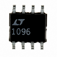
LTC1096CS8#PBF Linear Technology, LTC1096CS8#PBF Datasheet - Page 11

LTC1096CS8#PBF
Manufacturer Part Number
LTC1096CS8#PBF
Description
IC A/D CONV 8BIT SRL IN/OUT8SOIC
Manufacturer
Linear Technology
Datasheet
1.LTC1098CS8PBF.pdf
(32 pages)
Specifications of LTC1096CS8#PBF
Number Of Bits
8
Sampling Rate (per Second)
33k
Data Interface
Serial
Number Of Converters
1
Power Dissipation (max)
600µW
Voltage Supply Source
Single Supply
Operating Temperature
0°C ~ 70°C
Mounting Type
Surface Mount
Package / Case
8-SOIC (0.154", 3.90mm Width)
Number Of Elements
1
Resolution
8Bit
Architecture
SAR
Sample Rate
33KSPS
Input Polarity
Unipolar
Input Type
Voltage
Rated Input Volt
5V
Differential Input
Yes
Power Supply Requirement
Single
Single Supply Voltage (typ)
5V
Single Supply Voltage (min)
3V
Single Supply Voltage (max)
9V
Dual Supply Voltage (typ)
Not RequiredV
Dual Supply Voltage (min)
Not RequiredV
Dual Supply Voltage (max)
Not RequiredV
Power Dissipation
500mW
Differential Linearity Error
±1LSB(Typ)
Integral Nonlinearity Error
±1LSB
Operating Temp Range
0C to 70C
Operating Temperature Classification
Commercial
Mounting
Surface Mount
Pin Count
8
Package Type
SOIC N
Lead Free Status / RoHS Status
Lead free / RoHS Compliant
Available stocks
Company
Part Number
Manufacturer
Quantity
Price
PIN FUNCTIONS
LTC1096/LTC1096L
CS/SHDN (Pin 1): Chip Select Input. A logic low on this
input enables the LTC1096/LTC1096L. A logic high on this
input disables the LTC1096/LTC1096L and disconnects the
power to the LTC1096/LTC1096L.
IN
with respect to GND.
IN
with respect to GND.
GND (Pin 4): Analog Ground. GND should be tied directly
to an analog ground plane.
V
the span of the A/D converter and must be kept free of
noise with respect to GND.
D
result is shifted out of this output.
CLK (Pin 7): Shift Clock. This clock synchronizes the se-
rial data transfer.
V
to the A/D converter. It must be free of noise and ripple by
bypassing directly to the analog ground plane.
CC
REF
OUT
+
–
(Pin 2): Analog Input. This input must be free of noise
(Pin 3): Analog Input. This input must be free of noise
(Pin 8): Power Supply Voltage. This pin provides power
(Pin 5): Reference Input. The reference input defi nes
(Pin 6): Digital Data Output. The A/D conversion
LTC1098/LTC1098L
CS/SHDN (Pin 1): Chip Select Input. A logic low on this
input enables the LTC1098/LTC1098L. A logic high on this
input disables the LTC1098/LTC1098L and disconnects the
power to the LTC1098/LTC1098L.
CH0 (Pin 2): Analog Input. This input must be free of noise
with respect to GND.
CH1 (Pin 3): Analog Input. This input must be free of noise
with respect to GND.
GND (Pin 4): Analog Ground. GND should be tied directly
to an analog ground plane.
D
is shifted into this pin.
D
result is shifted out of this output.
CLK (Pin 7): Shift Clock. This clock synchronizes the se-
rial data transfer.
V
power and defi nes the span of the A/D converter. It must
be free of noise and ripple by bypassing directly to the
analog ground plane.
CC
IN
OUT
(V
(Pin 5): Digital Data Input. The multiplexer address
(Pin 6): Digital Data Output. The A/D conversion
REF
)(Pin 8): Power Supply Voltage. This pin provides
LTC1096/LTC1096L
LTC1098/LTC1098L
11
10968fc


