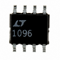
LTC1096CS8#PBF Linear Technology, LTC1096CS8#PBF Datasheet - Page 7

LTC1096CS8#PBF
Manufacturer Part Number
LTC1096CS8#PBF
Description
IC A/D CONV 8BIT SRL IN/OUT8SOIC
Manufacturer
Linear Technology
Datasheet
1.LTC1098CS8PBF.pdf
(32 pages)
Specifications of LTC1096CS8#PBF
Number Of Bits
8
Sampling Rate (per Second)
33k
Data Interface
Serial
Number Of Converters
1
Power Dissipation (max)
600µW
Voltage Supply Source
Single Supply
Operating Temperature
0°C ~ 70°C
Mounting Type
Surface Mount
Package / Case
8-SOIC (0.154", 3.90mm Width)
Number Of Elements
1
Resolution
8Bit
Architecture
SAR
Sample Rate
33KSPS
Input Polarity
Unipolar
Input Type
Voltage
Rated Input Volt
5V
Differential Input
Yes
Power Supply Requirement
Single
Single Supply Voltage (typ)
5V
Single Supply Voltage (min)
3V
Single Supply Voltage (max)
9V
Dual Supply Voltage (typ)
Not RequiredV
Dual Supply Voltage (min)
Not RequiredV
Dual Supply Voltage (max)
Not RequiredV
Power Dissipation
500mW
Differential Linearity Error
±1LSB(Typ)
Integral Nonlinearity Error
±1LSB
Operating Temp Range
0C to 70C
Operating Temperature Classification
Commercial
Mounting
Surface Mount
Pin Count
8
Package Type
SOIC N
Lead Free Status / RoHS Status
Lead free / RoHS Compliant
Available stocks
Company
Part Number
Manufacturer
Quantity
Price
DIGITAL AND DC ELECTRICAL CHARACTERISTICS
AC CHARACTERISTICS
LTC1096L/LTC1098L
The
V
SYMBOL
V
V
I
I
V
V
I
I
I
I
I
LTC1096/LTC1098
The
V
SYMBOL
t
f
t
t
t
t
t
t
t
C
IH
IL
OZ
SOURCE
SINK
REF
CC
SMPL
SMPL(MAX)
CONV
dDO
dis
en
hDO
f
r
IH
IL
OH
OL
IN
CC
CC
= 2.65V, V
= 5V, V
l
l
denotes the specifi cations which apply over the full operating temperature range, otherwise specifi cations are at T
denotes the specifi cations which apply over the full operating temperature range, otherwise specifi cations are at T
REF
PARAMETER
High Level Input Voltage
Low Level Input Voltage
High Level Input Current
Low Level Input Current
High Level Output Voltage
Low Level Output Voltage
Hi-Z Output Leakage
Output Source Current
Output Sink Current
Reference Current
Supply Current
PARAMETER
Analog Input Sample Time
Maximum Sampling Frequency
Conversion Time
Delay Time, CLK↓ to D
Delay Time, CS↑ to D
Delay Time, CLK↓ to D
Time Output Data Remains Valid After CLK↓
D
D
Input Capacitance
OUT
OUT
REF
= 5V, f
Fall Time
Rise Time
= 2.5V, f
CLK
= 500kHz, unless otherwise noted.
CLK
= 250kHz, unless otherwise noted.
OUT
OUT
OUT
Hi-Z
Data Valid
Enable
CONDITIONS
V
V
V
V
V
V
V
CS ≥ High
V
V
CS = V
t
t
CS = V
LTC1096L, t
LTC1096L, t
LTC1098L, t
LTC1098L, t
CYC
CYC
CC
CC
IN
IN
CC
CC
CC
OUT
OUT
= V
= 0V
= 3.6V
= 2.65V
= 2.65V, I
= 2.65V, I
= 2.65V, I
≥ 200μs, f
= 58μs, f
= 0V
= V
CC
CC
CC
CC
CYC
CYC
CYC
CYC
CONDITIONS
See Operating Sequence
See Operating Sequence
See Test Circuits
See Test Circuits
See Test Circuits
C
See Test Circuits
See Test Circuits
Analog Inputs On Channel
Analog Inputs Off Channel
Digital Input
O
O
O
CLK
LOAD
CLK
= 10μA
= 360μA
= 400μA
≥ 200μs, f
= 58μs, f
≥ 200μs, f
= 58μs, f
= 250kHz
≤ 50kHz
= 100pF
CLK
CLK
CLK
CLK
= 250kHz
= 250kHz
≤ 50kHz
≤ 50kHz
l
l
l
l
l
l
l
l
l
l
l
l
l
l
l
l
l
l
l
l
l
l
LTC1096/LTC1096L
LTC1098/LTC1098L
MIN
MIN
1.9
2.3
2.1
33
35.000
0.001
2.64
2.50
0.001
3.500
TYP
TYP
–10
120
155
200
170
180
1.5
15
40
44
60
70
25
25
8
5
5
MAX
MAX
0.45
–2.5
±3.0
50.0
450
450
250
250
100
180
230
2.5
0.3
3.0
80
88
2.5
7.5
A
A
= 25°C.
= 25°C.
CLK Cycles
CLK Cycles
UNITS
UNITS
10968fc
7
kHz
mA
mA
μA
μA
μA
μA
μA
μA
μA
μA
μA
μA
μA
ns
ns
ns
ns
ns
ns
pF
pF
pF
V
V
V
V
V


