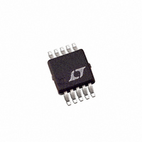
LTC1407CMSE#PBF Linear Technology, LTC1407CMSE#PBF Datasheet - Page 4

LTC1407CMSE#PBF
Manufacturer Part Number
LTC1407CMSE#PBF
Description
IC ADC 12BIT 3MSPS 10-MSOP
Manufacturer
Linear Technology
Datasheet
1.LTC1407CMSEPBF.pdf
(24 pages)
Specifications of LTC1407CMSE#PBF
Number Of Bits
12
Sampling Rate (per Second)
3M
Data Interface
Serial, SPI™
Number Of Converters
1
Power Dissipation (max)
14mW
Voltage Supply Source
Single Supply
Operating Temperature
0°C ~ 70°C
Mounting Type
Surface Mount
Package / Case
10-TFSOP, 10-MSOP (0.118", 3.00mm Width) Exposed Pad
Lead Free Status / RoHS Status
Lead free / RoHS Compliant
Available stocks
Company
Part Number
Manufacturer
Quantity
Price
DIGITAL INPUTS AND DIGITAL OUTPUTS
POWER REQUIREMENTS
LTC1407/LTC1407A
full operating temperature range, otherwise specifi cations are at T
SYMBOL
V
V
I
C
V
V
I
C
I
I
range, otherwise specifi cations are at T
TIMING CHARACTERISTICS
range, otherwise specifi cations are at T
SYMBOL
V
I
PD
SYMBOL
f
t
t
t
t
t
t
t
t
t
4
IN
OZ
SOURCE
SINK
DD
SAMPLE(MAX)
THROUGHPUT
SCK
CONV
1
2
3
4
5
6
IH
IL
IN
OH
OL
OZ
DD
PARAMETER
Maximum Sampling Frequency per Channel
(Conversion Rate)
Minimum Sampling Period (Conversion + Acquisiton Period)
Clock Period
Conversion Time
Minimum Positive or Negative SCLK Pulse Width
CONV to SCK Setup Time
SCK Before CONV
Minimum Positive or Negative CONV Pulse Width
SCK to Sample Mode
CONV to Hold Mode
PARAMETER
High Level Input Voltage
Low Level Input Voltage
Digital Input Current
Digital Input Capacitance
High Level Output Voltage
Low Level Output Voltage
Hi-Z Output Leakage D
Hi-Z Output Capacitance D
Output Short-Circuit Source Current
Output Short-Circuit Sink Current
PARAMETER
Supply Voltage
Supply Current
OUT
OUT
A
A
= 25°C. With internal reference, V
= 25°C. V
CONDITIONS
Active Mode, f
Active Mode (LTC1407H/LTC1407AH)
Nap Mode
Nap Mode (LTC1407H/LTC1407AH)
Sleep Mode (LTC1407/LTC1407H)
Sleep Mode (LTC1407A/LTC1407AH)
Active Mode with SCK in Fixed State (Hi or Lo)
The
DD
The
= 3V.
l
CONDITIONS
V
V
V
V
V
V
V
V
V
denotes the specifi cations which apply over the full operating temperature
l
DD
DD
IN
DD
DD
DD
OUT
OUT
OUT
denotes the specifi cations which apply over the full operating temperature
= 0V to V
= 3.3V
= 2.7V
= 3V, I
= 2.7V, I
= 2.7V, I
SAMPLE
= 0V to V
= 0V, V
= V
DD
OUT
= 3V
A
DD
OUT
OUT
= 1.5Msps
DD
= 25°C. V
= –200μA
DD
= 3V
CONDITIONS
(Note 16)
(Note 6)
(Note 6)
(Notes 6, 10)
(Note 6)
(Note 6)
(Note 6)
(Notes 6, 11)
= 160μA
= 1.6mA
DD
DD
The
= 3V.
= 3V.
l
denotes the specifi cations which apply over the
l
l
l
l
l
l
l
l
l
l
l
l
l
19.6
MIN
1.5
1.2
32
2
3
0
4
4
MIN
MIN
2.4
2.5
2.7
TYP
34
0.05
0.10
TYP
TYP
2.9
4.7
5.2
1.1
1.2
2.0
2.0
20
15
12
5
1
10000
10000
MAX
667
MAX
MAX
±10
±10
0.6
0.4
3.6
7.0
8.0
1.5
1.8
15
10
SCLK cycles
UNITS
UNITS
UNITS
1407fb
MHz
mW
mA
mA
mA
mA
mA
mA
μA
μA
μA
μA
ns
ns
ns
ns
ns
ns
ns
ns
pF
pF
V
V
V
V
V
V


