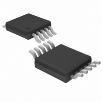
LTC2411IMS#PBF Linear Technology, LTC2411IMS#PBF Datasheet - Page 12

LTC2411IMS#PBF
Manufacturer Part Number
LTC2411IMS#PBF
Description
IC A/D CONV 24BIT MICRPWR 10MSOP
Manufacturer
Linear Technology
Datasheet
1.LTC2411CMSPBF.pdf
(40 pages)
Specifications of LTC2411IMS#PBF
Number Of Bits
24
Sampling Rate (per Second)
7.5
Data Interface
MICROWIRE™, Serial, SPI™
Number Of Converters
2
Power Dissipation (max)
1mW
Voltage Supply Source
Single Supply
Operating Temperature
-40°C ~ 85°C
Mounting Type
Surface Mount
Package / Case
10-TFSOP, 10-MSOP (0.118", 3.00mm Width)
Number Of Elements
1
Resolution
24Bit
Architecture
Delta-Sigma
Sample Rate
0.008KSPS
Input Polarity
Bipolar
Input Type
Voltage
Rated Input Volt
±2.75V
Differential Input
Yes
Power Supply Requirement
Single
Single Supply Voltage (typ)
3.3/5V
Single Supply Voltage (min)
2.7V
Single Supply Voltage (max)
5.5V
Dual Supply Voltage (typ)
Not RequiredV
Dual Supply Voltage (min)
Not RequiredV
Dual Supply Voltage (max)
Not RequiredV
Integral Nonlinearity Error
14ppm of Vref
Operating Temp Range
-40C to 85C
Operating Temperature Classification
Industrial
Mounting
Surface Mount
Pin Count
10
Package Type
MSOP
Input Signal Type
Differential
Lead Free Status / RoHS Status
Lead free / RoHS Compliant
Available stocks
Company
Part Number
Manufacturer
Quantity
Price
APPLICATIO S I FOR ATIO
LTC2411/LTC2411-1
integrity of the conversion result and of the serial interface
mode selection. (See the 2-wire I/O sections in the Serial
Interface Timing Modes section.)
When the V
the converter creates an internal power-on-reset (POR)
signal with a duration of approximately 1ms. The POR
signal clears all internal registers. Following the POR
signal, the LTC2411/LTC2411-1 start a normal conversion
cycle and follow the succession of states described above.
The first conversion result following POR is accurate
within the specifications of the device if the power supply
voltage is restored within the operating range (2.7V to
5.5V) before the end of the POR time interval.
Reference Voltage Range
The LTC2411/LTC2411-1 accept a truly differential exter-
nal reference voltage. The absolute/common mode volt-
age specification for the REF
entire range from GND to V
operation, the REF
the REF
The LTC2411/LTC2411-1 can accept a differential refer-
ence voltage from 0.1V to V
is determined by the thermal noise of the front-end cir-
cuits, and, as such, its value in nanovolts is nearly constant
with reference voltage. A decrease in reference voltage will
not significantly improve the converter’s effective resolu-
tion. On the other hand, a reduced reference voltage will
improve the converter’s overall INL performance. A reduced
reference voltage will also improve the converter perfor-
mance when operated with an external conversion clock
(external F
Input Voltage Range
The analog input is truly differential with an absolute/
common mode range for the IN
extending from GND – 0.3V to V
these limits, the ESD protection devices begin to turn on
and the errors due to input leakage current increase
rapidly. Within these limits, the LTC2411/LTC2411-1 con-
vert the bipolar differential input signal, V
from – FS = – 0.5 • V
REF
12
+
– REF
–
pin.
O
signal) at substantially higher output data rates.
CC
–
. Outside this range the converter indicates
voltage rises above this critical threshold,
+
U
pin must always be more positive than
REF
to +FS = 0.5 • V
U
CC
+
. The converter output noise
CC
and REF
. For correct converter
+
W
CC
and IN
–
REF
+ 0.3V. Outside
pins covers the
IN
where V
–
= IN
input pins
U
+
– IN
REF
–
=
,
the overrange or the underrange condition using distinct
output codes.
Input signals applied to IN
300mV below ground and above V
fault current, resistors of up to 5k may be added in series
with the IN
mance of the device. In the physical layout, it is important
to maintain the parasitic capacitance of the connection
between these series resistors and the corresponding pins
as low as possible; therefore, the resistors should be
located as close as practical to the pins. In addition, series
resistors will introduce a temperature dependent offset
error due to the input leakage current. A 1nA input leakage
current will develop a 1ppm offset error on a 5k resistor if
V
dependency.
Output Data Format
The LTC2411/LTC2411-1 serial output data stream is 32
bits long. The first 3 bits represent status information in-
dicating the sign and conversion state. The next 24 bits are
the conversion result, MSB first. The remaining 5 bits are
sub LSBs beyond the 24-bit level that may be included in
averaging or discarded without loss of resolution. The third
and fourth bits together are also used to indicate an
underrange condition (the differential input voltage is be-
low – FS) or an overrange condition (the differential input
voltage is above + FS).
Bit 31 (first output bit) is the end of conversion (EOC)
indicator. This bit is available at the SDO pin during the
conversion and sleep states whenever the CS pin is LOW.
This bit is HIGH during the conversion and goes LOW
when the conversion is complete.
Bit 30 (second output bit) is a dummy bit (DMY) and is
always LOW.
Bit 29 (third output bit) is the conversion result sign indi-
cator (SIG). If V
bit is LOW.
Bit 28 (fourth output bit) is the most significant bit (MSB)
of the result. This bit in conjunction with Bit 29 also
provides the underrange or overrange indication. If both
Bit 29 and Bit 28 are HIGH, the differential input voltage is
REF
= 5V. This error has a very strong temperature
+
and IN
IN
is >0, this bit is HIGH. If V
–
pins without affecting the perfor-
+
and IN
CC
–
. In order to limit any
pins may extend by
IN
is <0, this


