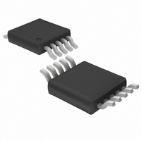
LTC2411IMS#PBF Linear Technology, LTC2411IMS#PBF Datasheet - Page 27

LTC2411IMS#PBF
Manufacturer Part Number
LTC2411IMS#PBF
Description
IC A/D CONV 24BIT MICRPWR 10MSOP
Manufacturer
Linear Technology
Datasheet
1.LTC2411CMSPBF.pdf
(40 pages)
Specifications of LTC2411IMS#PBF
Number Of Bits
24
Sampling Rate (per Second)
7.5
Data Interface
MICROWIRE™, Serial, SPI™
Number Of Converters
2
Power Dissipation (max)
1mW
Voltage Supply Source
Single Supply
Operating Temperature
-40°C ~ 85°C
Mounting Type
Surface Mount
Package / Case
10-TFSOP, 10-MSOP (0.118", 3.00mm Width)
Number Of Elements
1
Resolution
24Bit
Architecture
Delta-Sigma
Sample Rate
0.008KSPS
Input Polarity
Bipolar
Input Type
Voltage
Rated Input Volt
±2.75V
Differential Input
Yes
Power Supply Requirement
Single
Single Supply Voltage (typ)
3.3/5V
Single Supply Voltage (min)
2.7V
Single Supply Voltage (max)
5.5V
Dual Supply Voltage (typ)
Not RequiredV
Dual Supply Voltage (min)
Not RequiredV
Dual Supply Voltage (max)
Not RequiredV
Integral Nonlinearity Error
14ppm of Vref
Operating Temp Range
-40C to 85C
Operating Temperature Classification
Industrial
Mounting
Surface Mount
Pin Count
10
Package Type
MSOP
Input Signal Type
Differential
Lead Free Status / RoHS Status
Lead free / RoHS Compliant
Available stocks
Company
Part Number
Manufacturer
Quantity
Price
APPLICATIO S I FOR ATIO
user is thus advised to minimize the combined source
impedance driving the REF
try to match it.
The magnitude of the dynamic reference current depends
upon the size of the very stable internal sampling capaci-
tors and upon the accuracy of the converter sampling
clock. The accuracy of the internal clock over the entire
temperature and power supply range is typical better than
1%. Such a specification can also be easily achieved by an
external clock. When relatively stable resistors (50ppm/ C)
are used for the external source impedance seen by REF
and REF
error will be insignificant (about 1% of its value over the
entire temperature and voltage range). Even for the most
stringent applications, a one-time calibration operation
may be sufficient.
In addition to the reference sampling charge, the reference
pins ESD protection diodes have a temperature dependent
leakage current. This leakage current, nominally 1nA
( 10nA max), results in a small gain error. A 100 source
resistance will create a 0.05 V typical and 0.5 V maxi-
mum full-scale error.
Output Data Rate
When using its internal oscillator, the LTC2411 can pro-
duce up to 7.5 readings per second with a notch frequency
of 60Hz (F
notch frequency of 50Hz (F
can produce up to 6.8 readings per second with F
The actual output data rate will depend upon the length of
the sleep and data output phases which are controlled by
the user and which can be made insignificantly short.
When operated with an external conversion clock (F
connected to an external oscillator), the LTC2411/LTC2411-
1 output data rate can be increased as desired. The
duration of the conversion phase is 20510/f
= 153600Hz, the converter behaves as if the internal
oscillator is used and the notch is set at 60Hz. There is no
significant difference in the LTC2411/LTC2411-1 perfor-
mance between these two operation modes.
An increase in f
translate into a proportional increase in the maximum
output data rate. This substantial advantage is nevertheless
–
, the expected drift of the dynamic current gain
O
= LOW) and 6.25 readings per second with a
EOSC
U
over the nominal 153600Hz will
U
+
O
and REF
= HIGH) and the LTC2411-1
W
–
pins rather than to
EOSC
U
O
. If f
= LOW.
EOSC
O
+
accompanied by three potential effects, which must be
carefully considered.
First, a change in f
in the internal notch position and in a reduction of the
converter differential mode rejection at the power line
frequency. In many applications, the subsequent perfor-
mance degradation can be substantially reduced by rely-
ing upon the LTC2411/LTC2411-1’s exceptional common
mode rejection and by carefully eliminating common
mode to differential mode conversion sources in the input
circuit. The user should avoid single-ended input filters
and should maintain a very high degree of matching and
symmetry in the circuits driving the IN
Second, the increase in clock frequency will increase
proportionally the amount of sampling charge transferred
through the input and the reference pins. If large external
input and/or reference capacitors (C
previous section provides formulae for evaluating the
effect of the source resistance upon the converter perfor-
mance for any value of f
or reference capacitors (C
the external source resistance upon the LTC2411/
LTC2411-1 typical performance can be inferred from
Figures 13, 14 and 17 in which the horizontal axis is scaled
by 153600/f
Third, an increase in the frequency of the external oscilla-
tor above 460800Hz (a more than 3 increase in the output
data rate) will start to decrease the effectiveness of the
internal autocalibration circuits. This will result in a progres-
sive degradation in the converter accuracy and linearity.
Typical measured performance curves for output data rates
up to 100 readings per second are shown in Figures 20 to
27. In order to obtain the highest possible level of accuracy
from this converter at output data rates above 20 readings
per second, the user is advised to maximize the power
supply voltage used and to limit the maximum ambient
operating temperature. In certain circumstances, a reduc-
tion of the differential reference voltage may be beneficial.
Input Bandwidth
The combined effect of the internal sinc
of the analog and digital autocalibration circuits deter-
mines the LTC2411/LTC2411-1 input bandwidth. When
EOSC
LTC2411/LTC2411-1
.
EOSC
will result in a proportional change
EOSC
IN
, C
. If small external input and/
REF
) are used, the effect of
IN
, C
+
4
REF
and IN
digital filter and
) are used, the
–
pins.
27


