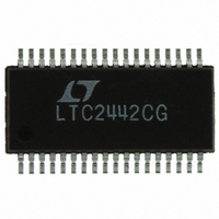
LTC2442CG#PBF Linear Technology, LTC2442CG#PBF Datasheet - Page 9

LTC2442CG#PBF
Manufacturer Part Number
LTC2442CG#PBF
Description
IC ADC 24BIT 4CH 36-SSOP
Manufacturer
Linear Technology
Datasheet
1.LTC2442CGPBF.pdf
(32 pages)
Specifications of LTC2442CG#PBF
Number Of Bits
24
Sampling Rate (per Second)
8k
Data Interface
MICROWIRE™, Serial, SPI™
Number Of Converters
1
Power Dissipation (max)
50mW
Voltage Supply Source
Single Supply
Operating Temperature
0°C ~ 70°C
Mounting Type
Surface Mount
Package / Case
36-SSOP (0.200", 5.30mm Width)
Lead Free Status / RoHS Status
Lead free / RoHS Compliant
Available stocks
Company
Part Number
Manufacturer
Quantity
Price
FU CTIO AL BLOCK DIAGRA
TEST CIRCUITS
APPLICATIO S I FOR ATIO
CONVERTER OPERATION
Converter Operation Cycle
The LTC2442 is a multi-channel, high speed, ΔΣ analog-
to-digital converter with an easy to use 3- or 4-wire serial
interface (see Figure 1). Its operation is made up of three
states. The converter operating cycle begins with the con-
version, followed by the sleep state and ends with the data
output/input (see Figure 2). The 4-wire interface consists
of serial data input (SDI), serial data output (SDO), serial
clock (SCK) and chip select (CS). The interface, timing,
operation cycle and data out format is compatible with
Linear’s entire family of ΔΣ converters.
Initially, the LTC2442 performs a conversion. Once the
conversion is complete, the device enters the sleep state.
The part remains in the sleep state as long as CS is HIGH.
The conversion result is held indefi nitely in a static shift
register while the converter is in the sleep state.
U
COM
GND
CH0
CH1
CH2
CH3
V
U
CC
SDO
U
MUX
Hi-Z TO V
V
V
1.69k
OL
OH
MUXOUTB
MUXOUTA +INA –INA
TO V
U
TO Hi-Z
OH
OH
+INB
C
LOAD
W
–INB
2442 TA03
= 20pF
–
+
+
–
V
+
AMPB
AMPA
V
Figure 1. Functional Block Diagram
–
OUTB
OUTA
U
W
ADCINB
ADCINA
IN
IN
REF
+
–
∆Σ MODULATOR
+
DIFFERENTIAL
3RD ORDER
REF
–
Figure 2. LTC2442 State Transition Diagram
AUTOCALIBRATION
DECIMATING FIR
AND CONTROL
ADDRESS
SDO
Hi-Z TO V
V
V
OH
OL
V
TO Hi-Z
TO V
OSR=256,1X MODE
IN
CHANNEL SELECT
CC
SPEED SELECT
DATA OUTPUT
+
OSCILLATOR
INTERFACE
1.69k
=CH0, IN
INTERNAL
POWER UP
C
OL
CONVERT
CS = LOW
OL
SERIAL
SCK
LOAD
SLEEP
AND
2442 F01
2442 TA04
= 20pF
–
=CH1
2442 F02
F
BUSY
SDI
SCK
SDO
CS
EXT
LTC2442
O
9
2442f


