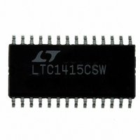
LTC1415CSW#PBF Linear Technology, LTC1415CSW#PBF Datasheet - Page 13

LTC1415CSW#PBF
Manufacturer Part Number
LTC1415CSW#PBF
Description
IC A/D CONV 12BIT SAMPLNG 28SOIC
Manufacturer
Linear Technology
Datasheet
1.LTC1415CSWPBF.pdf
(24 pages)
Specifications of LTC1415CSW#PBF
Number Of Bits
12
Sampling Rate (per Second)
1.25M
Data Interface
Parallel
Number Of Converters
1
Power Dissipation (max)
100mW
Voltage Supply Source
Single Supply
Operating Temperature
0°C ~ 70°C
Mounting Type
Surface Mount
Package / Case
28-SOIC (0.300", 7.50mm Width)
Number Of Elements
1
Resolution
12Bit
Architecture
SAR
Sample Rate
1.25MSPS
Input Polarity
Unipolar
Input Type
Voltage
Rated Input Volt
4.096V
Differential Input
Yes
Power Supply Requirement
Analog and Digital
Single Supply Voltage (typ)
5V
Single Supply Voltage (min)
4.75V
Single Supply Voltage (max)
5.25V
Dual Supply Voltage (typ)
Not RequiredV
Dual Supply Voltage (min)
Not RequiredV
Dual Supply Voltage (max)
Not RequiredV
Power Dissipation
100mW
Differential Linearity Error
±1LSB
Integral Nonlinearity Error
±1LSB
Operating Temp Range
0C to 70C
Operating Temperature Classification
Commercial
Mounting
Surface Mount
Pin Count
28
Package Type
SOIC W
Lead Free Status / RoHS Status
Lead free / RoHS Compliant
Available stocks
Company
Part Number
Manufacturer
Quantity
Price
APPLICATIONS
4.096V to 2.048V and shifts the common mode voltage
from half of full scale to 2.274V.
AC Coupled Inputs
The analog inputs can be AC coupled for applications
where the input has no DC information. The input of the
Figure 10c. 2.048V Input Range with a Common Mode
Voltage of 2.274V. For Low Distortion AC Applications
LT1004-1.2
V
OUT
80
70
60
50
40
30
20
10
Figure 10a. CMRR vs Input Frequency
= 1.2V
0
1k
1.25V TO 3.298V
ANALOG INPUT
24
U
Figure 10e. 2.048V
ANALOG INPUT
INPUT FREQUENCY (Hz)
10k
2.048V
INFORMATION
1 F
10 F
U
P-P
1
2
3
4
5
100k
+A
–A
V
REFCOMP
AGND
REF
IN
IN
LTC1415
W
1k
P-P
LTC1415 • F10c
LTC1415 • F10a
1M
Input Range with AC Coupling. For Low Distortion AC Applications
LT1004-1.2
1k
2M
+
–
U
25
9k
1 F
10 F
ADC does need to be DC biased at midscale. Figures 10d
and 10e demonstrate AC coupling and the required bias-
ing. Figure 10d shows the ADC with a full scale of 4.096V,
a common mode voltage of 2.048V and an input that
swings from 0V to 4.096V. This circuit has the lowest
noise (SINAD = 72dB to 100kHz) but will have distortion
1
2
3
4
5
Figure 10b. Shifting the Input Range Up from Ground by 200mV
+A
–A
V
REFCOMP
AGND
ANALOG INPUT
REF
IN
IN
LTC1415
4.096V
Figure 10d. 4.096V
For Low Noise AC Applications
LTC1415 • F10e
P-P
200
R1
ANALOG INPUT
0.2V TO 4.296V
2k
2k
R2
3.9k
10 F
1
2
3
4
5
10 F
P-P
+A
–A
V
REFCOMP
AGND
1
2
3
4
5
REF
Input Range with AC Coupling.
IN
IN
+A
–A
V
REFCOMP
AGND
LTC1415
REF
IN
IN
LTC1415
LTC1415 • F10b
LTC1415 • F10d
LTC1415
13


