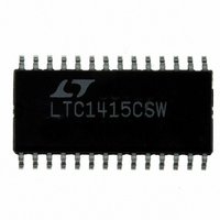
LTC1415CSW#PBF Linear Technology, LTC1415CSW#PBF Datasheet - Page 2

LTC1415CSW#PBF
Manufacturer Part Number
LTC1415CSW#PBF
Description
IC A/D CONV 12BIT SAMPLNG 28SOIC
Manufacturer
Linear Technology
Datasheet
1.LTC1415CSWPBF.pdf
(24 pages)
Specifications of LTC1415CSW#PBF
Number Of Bits
12
Sampling Rate (per Second)
1.25M
Data Interface
Parallel
Number Of Converters
1
Power Dissipation (max)
100mW
Voltage Supply Source
Single Supply
Operating Temperature
0°C ~ 70°C
Mounting Type
Surface Mount
Package / Case
28-SOIC (0.300", 7.50mm Width)
Number Of Elements
1
Resolution
12Bit
Architecture
SAR
Sample Rate
1.25MSPS
Input Polarity
Unipolar
Input Type
Voltage
Rated Input Volt
4.096V
Differential Input
Yes
Power Supply Requirement
Analog and Digital
Single Supply Voltage (typ)
5V
Single Supply Voltage (min)
4.75V
Single Supply Voltage (max)
5.25V
Dual Supply Voltage (typ)
Not RequiredV
Dual Supply Voltage (min)
Not RequiredV
Dual Supply Voltage (max)
Not RequiredV
Power Dissipation
100mW
Differential Linearity Error
±1LSB
Integral Nonlinearity Error
±1LSB
Operating Temp Range
0C to 70C
Operating Temperature Classification
Commercial
Mounting
Surface Mount
Pin Count
28
Package Type
SOIC W
Lead Free Status / RoHS Status
Lead free / RoHS Compliant
Available stocks
Company
Part Number
Manufacturer
Quantity
Price
A
A
LTC1415
AV
Supply Voltage (V
Analog Input Voltage (Note 3) ...... – 0.3V to V
Digital Input Voltage (Note 4) .................. – 0.3V to 12V
Digital Output Voltage .................... – 0.3V to V
Power Dissipation ............................................. 500mW
Operating Temperature Range
Storage Temperature Range ................ – 65 C to 150 C
Lead Temperature (Soldering, 10 sec)................. 300 C
CO
SYMBOL PARAMETER
V
I
C
t
t
t
CMRR
PARAMETER
Resolution (No Missing Codes)
Integral Linearity Error
Differential Linearity Error
Offset Error
Full-Scale Error
Full-Scale Tempco
2
IN
jitter
ACQ
AP
IN
IN
BSOLUTE
U
DD
LTC1415C .............................................. 0 C to 70 C
LTC1415I ........................................... – 40 C to 85 C
A
U
= DV
LOG
VERTER
Analog Input Range (Note 9)
Analog Input Leakage Current
Analog Input Capacitance
Sample-and-Hold Acquisition Time
Sample-and-Hold Aperture Delay Time
Sample-and-Hold Aperture Delay Time Jitter
Analog Input Common Mode Rejection Ratio
DD
=OV
DD
I
U
= V
DD
W
PUT
) ................................................ 6V
DD
C
A
(Notes 1, 2)
HARA TERISTICS
XI
W
(Note 5)
U
C
W
R
A
TI
U
DD
DD
G
CONDITIONS
4.75V V
CS = High
Between Conversions
During Conversions
0V < V
CONDITIONS
(Note 7)
(Note 8)
I
OUT(REF)
+ 0.3V
+ 0.3V
S
With Internal Reference (Notes 5, 6)
CM
= 0
DD
< V
DD
5.25V
, DC to MHz
Consult factory for Military grade parts.
PACKAGE/ORDER I FOR ATIO
D11 (MSB)
28-LEAD PLASTIC SSOP
REFCOMP
DGND
AGND
+A
–A
V
G PACKAGE
D10
REF
D9
D8
D7
D6
D5
D4
IN
IN
T
T
JMAX
JMAX
10
11
12
13
14
1
2
3
4
5
6
7
8
9
= 110 C,
= 110 C,
TOP VIEW
JA
JA
28-LEAD PLASTIC SO WIDE
= 95 C/W (G)
= 130 C/W (SW)
SW PACKAGE
28
27
26
25
24
23
22
21
20
19
18
17
16
15
AV
DV
OV
BUSY
CS
CONVST
RD
SHDN
NAP/SLP
OGND
D0
D1
D2
D3
MIN
MIN
12
DD
DD
DD
U
4.096
0.35
0.25
–1.5
TYP
TYP
19
50
60
2
15
5
1
PART NUMBER
W
LTC1415CG
LTC1415CSW
LTC1415IG
LTC1415ISW
ORDER
MAX
MAX
150
20
1
1
1
6
8
ppm/ C
UNITS
UNITS
ps
U
LSB
LSB
LSB
LSB
LSB
RMS
Bits
dB
pF
pF
ns
ns
V
A


