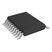
AD7908BRUZ Analog Devices Inc, AD7908BRUZ Datasheet - Page 20

AD7908BRUZ
Manufacturer Part Number
AD7908BRUZ
Description
IC ADC 8BIT 8CH 1MSPS 20-TSSOP
Manufacturer
Analog Devices Inc
Specifications of AD7908BRUZ
Data Interface
DSP, MICROWIRE™, QSPI™, Serial, SPI™
Number Of Bits
8
Sampling Rate (per Second)
1M
Number Of Converters
1
Power Dissipation (max)
13.5mW
Voltage Supply Source
Single Supply
Operating Temperature
-40°C ~ 85°C
Mounting Type
Surface Mount
Package / Case
20-TSSOP (0.173", 4.40mm Width)
Resolution (bits)
8bit
Sampling Rate
1MSPS
Input Channel Type
Single Ended
Supply Voltage Range - Analog
2.7V To 5.25V
Supply Current
2.7mA
Digital Ic Case Style
TSSOP
Lead Free Status / RoHS Status
Lead free / RoHS Compliant
For Use With
EVAL-AD79X8CBZ - BOARD EVALUATION FOR AD79X8
Lead Free Status / RoHS Status
Lead free / RoHS Compliant, Lead free / RoHS Compliant
Available stocks
Company
Part Number
Manufacturer
Quantity
Price
Company:
Part Number:
AD7908BRUZ
Manufacturer:
ADI
Quantity:
1 000
Part Number:
AD7908BRUZ
Manufacturer:
ADI/亚德诺
Quantity:
20 000
Company:
Part Number:
AD7908BRUZ-REEL
Manufacturer:
ADI
Quantity:
1 000
AD7908/AD7918/AD7928
0V TO REF
Analog Input Selection
Any one of eight analog input channels can be selected for
conversion by programming the multiplexer with the Address
Bit ADD2 to Address Bit ADD0 in the control register. The
channel configurations are shown in Table 8. The AD7908/
AD7918/AD7928 can also be configured to automatically cycle
through a number of channels as selected. The sequencer
feature is accessed via the SEQ and SHADOW bits in the
control register (see Table 10).
The AD7908/AD7918/AD7928 can be programmed to
continuously convert on a selection of channels in ascending
order. The analog input channels to be converted on are
selected through programming the relevant bits in the
SHADOW register (see the SHADOW Register section). The
next serial transfer then acts on the sequence programmed by
executing a conversion on the lowest channel in the selection.
The next serial transfer results in a conversion on the next
highest channel in the sequence, and so on.
It is not necessary to write to the control register once a
sequencer operation has been initiated. The WRITE bit must be
set to zero or the DIN line tied low to ensure the control register
is not accidentally overwritten, or the sequence operation
interrupted. If the control register is written to at any time
NOTE
1. ALL UNUSED INPUT CHANNELS SHOULD BE CONNECTED TO AGND.
IN
0.1µF
V
V
AGND
IN
IN
0
7
AV
•
•
Figure 20. Typical Connection Diagram
DD
0.1µF
REF
0V
V
AD7908/
AD7918/
AD7928
IN
AD780
10µF
2.5V
V
DRIVE
SUPPLY
DOUT
SCLK
0.1µF
5V
DIN
CS
V
0.1µF
INTERFACE
10µF
R3
R2
SERIAL
R1 = R2 = R3 = R4
V
R4
R1
Figure 19. Handling Bipolar Signals
REF
SUPPLY
µC/µP
3V
Rev. B | Page 20 of 28
REF
V
V
IN
IN
•
•
0
7
AD7908/
AD7918/
AD7928
IN
AV
DD
during the sequence, then it must be ensured that the SEQ and
SHADOW bits are set to 1, 0 to avoid interrupting the
automatic conversion sequence. This pattern continues until
such time as the AD7908/AD7918/AD7928 is written to and the
SEQ and SHADOW bits are configured with any bit combination
except 1, 0. On completion of the sequence, the AD7908/
AD7918/AD7928 sequencer returns to the first selected channel
in the SHADOW register and commence the sequence again.
Rather than selecting a particular sequence of channels, a
number of consecutive channels beginning with Channel 0 can
also be programmed via the control register alone, without
needing to write to the SHADOW register. This is possible if the
SEQ and SHADOW bits are set to 1,1. The channel address bits
ADD2 through ADD0 then determine the final channel in the
consecutive sequence. The next conversion is on Channel 0,
then Channel 1, and so on until the channel selected via the
address bits ADD2 through ADD0 is reached. The cycle begins
again on the next serial transfer, provided the WRITE bit is set
to low, or if high, that the SEQ and SHADOW bits are set to
1, 0; then the ADC continues its preprogrammed automatic
sequence uninterrupted.
Regardless of which channel selection method is used, the 16-bit
word output from the AD7928 during each conversion always
contains a leading zero, three channel address bits that the
conversion result corresponds to, followed by the 12-bit
conversion result. The AD7918 outputs a leading zero, three
channel address bits that the conversion result corresponds to,
followed by the 10-bit conversion result and two trailing zeros;
the AD7908 outputs a leading zero, three channel address bits
that the conversion result corresponds to, followed by the 8-bit
conversion result and four trailing zeros. (See the Serial
Interface section.)
Digital Inputs
The digital inputs applied to the AD7908/AD7918/AD7928 are
not limited by the maximum ratings that limit the analog
V
DOUT
DRIVE
TWOS COMPLEMENT
+REF
REF
–REF
IN
IN
IN
(= 0V)
(= 2 × REF
IN)
DSP/µP
V
V
DD
DD
011…111
000…000
100…000


