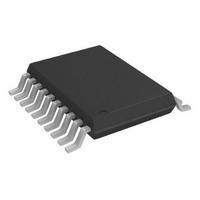
AD7908BRUZ Analog Devices Inc, AD7908BRUZ Datasheet - Page 24

AD7908BRUZ
Manufacturer Part Number
AD7908BRUZ
Description
IC ADC 8BIT 8CH 1MSPS 20-TSSOP
Manufacturer
Analog Devices Inc
Specifications of AD7908BRUZ
Data Interface
DSP, MICROWIRE™, QSPI™, Serial, SPI™
Number Of Bits
8
Sampling Rate (per Second)
1M
Number Of Converters
1
Power Dissipation (max)
13.5mW
Voltage Supply Source
Single Supply
Operating Temperature
-40°C ~ 85°C
Mounting Type
Surface Mount
Package / Case
20-TSSOP (0.173", 4.40mm Width)
Resolution (bits)
8bit
Sampling Rate
1MSPS
Input Channel Type
Single Ended
Supply Voltage Range - Analog
2.7V To 5.25V
Supply Current
2.7mA
Digital Ic Case Style
TSSOP
Lead Free Status / RoHS Status
Lead free / RoHS Compliant
For Use With
EVAL-AD79X8CBZ - BOARD EVALUATION FOR AD79X8
Lead Free Status / RoHS Status
Lead free / RoHS Compliant, Lead free / RoHS Compliant
Available stocks
Company
Part Number
Manufacturer
Quantity
Price
Company:
Part Number:
AD7908BRUZ
Manufacturer:
ADI
Quantity:
1 000
Part Number:
AD7908BRUZ
Manufacturer:
ADI/亚德诺
Quantity:
20 000
Company:
Part Number:
AD7908BRUZ-REEL
Manufacturer:
ADI
Quantity:
1 000
AD7908/AD7918/AD7928
8/10/12 bits of data are preceded by a leading zero and the
3-channel address bits (ADD2 to ADD0) identify which
channel the result corresponds to. CS going low provides the
leading zero to be read in by the microcontroller or DSP. The
three remaining address bits and data bits are then clocked out
by subsequent SCLK falling edges beginning with the first
address bit (ADD2). Thus the first falling clock edge on the
serial clock has a leading zero provided and also clocks out
Address Bit ADD2. The final bit in the data transfer is valid on
the 16th falling edge, having been clocked out on the previous
(15th) falling edge.
Writing of information to the control register takes place on the
first 12 falling edges of SCLK in a data transfer, assuming the
MSB, that is, the WRITE bit, has been set to 1. If the control
register is programmed to use the SHADOW register, then
writing of information to the SHADOW register takes place on
all 16 SCLK falling edges in the next serial transfer, as shown for
example on the AD7928 in Figure 29. Two sequence options
can be programmed in the SHADOW register. If the user does
not want to program a second sequence, then the eight LSBs
should be filled with zeros. The SHADOW register is updated
upon the rising edge of CS and the track-and-hold begins to
track the first channel selected in the sequence.
The AD7908 outputs a leading zero and three channel address
bits that the conversion result corresponds to, followed by the
8-bit conversion result and four trailing zeros. The AD7918
outputs a leading zero and three channel address bits that the
conversion result corresponds to, followed by the 10-bit
conversion result and two trailing zeros. The 16-bit word read
from the AD7928 always contains a leading zero and three
channel address bits that the conversion result corresponds to,
followed by the 12-bit conversion result.
Rev. B | Page 24 of 28
MICROPROCESSOR INTERFACING
The serial interface on the AD7908/AD7918/AD7928 allows the
part to be directly connected to a range of many different
microprocessors. This section explains how to interface the
AD7908/AD7918/AD7928 with some of the more common
microcontroller and DSP serial interface protocols.
AD7908/AD7918/AD7928 to TMS320C541
The serial interface on the TMS320C541 uses a continuous
serial clock and frame synchronization signals to synchronize
the data transfer operations with peripheral devices like the
AD7908/AD7918/AD7928. The CS input allows easy
interfacing between the TMS320C541 and the AD7908/
AD7918/AD7928 without any glue logic required. The serial
port of the TMS320C541 is set up to operate in burst mode with
internal CLKX0 (Tx serial clock on Serial Port 0) and FSX0 (Tx
frame sync from Serial Port 0). The serial port control register
(SPC) must have the following setup: FO = 0, FSM = 1, MCM = 1,
and TXM = 1. The connection diagram is shown in Figure 30. It
should be noted that for signal processing applications, it is
imperative that the frame synchronization signal from the
TMS320C541 provides equidistant sampling. The V
the AD7908/AD7918/AD7928 takes the same supply voltage as
that of the TMS320C541. This allows the ADC to operate at a
higher voltage than the serial interface, that is, TMS320C541, if
necessary.
DRIVE
pin of


