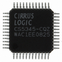
CS5345-CQZ Cirrus Logic Inc, CS5345-CQZ Datasheet - Page 27

CS5345-CQZ
Manufacturer Part Number
CS5345-CQZ
Description
IC ADC AUD 104DB 200KHZ 48-LQFP
Manufacturer
Cirrus Logic Inc
Specifications of CS5345-CQZ
Data Interface
Serial
Number Of Bits
24
Sampling Rate (per Second)
200k
Number Of Converters
2
Power Dissipation (max)
485mW
Voltage Supply Source
Analog and Digital
Operating Temperature
-10°C ~ 70°C
Mounting Type
Surface Mount
Package / Case
48-LQFP
Resolution (bits)
24bit
Sampling Rate
192kSPS
Input Channel Type
Single Ended
Supply Voltage Range - Analog
3.13V To 5.25V
Supply Current
41mA
Digital Ic Case Style
QFP
Lead Free Status / RoHS Status
Lead free / RoHS Compliant
For Use With
598-1780 - EVALUATION BOARD FOR CS5345
Lead Free Status / RoHS Status
Lead free / RoHS Compliant, Lead free / RoHS Compliant
Other names
598-1083
Available stocks
Company
Part Number
Manufacturer
Quantity
Price
Company:
Part Number:
CS5345-CQZ
Manufacturer:
QFP
Quantity:
513
Part Number:
CS5345-CQZ
Manufacturer:
CIRRUS
Quantity:
20 000
Company:
Part Number:
CS5345-CQZR
Manufacturer:
Cirrus Logic Inc
Quantity:
10 000
DS658F2
SCL
SDA
SDA
SCL
START
START
be connected through a resistor to VLC or DGND as desired. The state of the pins is sensed while the
CS5345 is being reset.
The signal timings for a read and write cycle are shown in
defined as a falling transition of SDA while the clock is high. A Stop condition is a rising transition while
the clock is high. All other transitions of SDA occur while the clock is low. The first byte sent to the CS5345
after a Start condition consists of a 7-bit chip address field and a R/W bit (high for a read, low for a write).
The upper 5 bits of the 7-bit address field are fixed at 10011. To communicate with a CS5345, the chip
address field, which is the first byte sent to the CS5345, should match 10011 followed by the settings of
the AD1 and AD0. The eighth bit of the address is the R/W bit. If the operation is a write, the next byte is
the Memory Address Pointer (MAP) which selects the register to be read or written. If the operation is a
read, the contents of the register pointed to by the MAP will be output. Following each data byte, the mem-
ory address pointer will automatically increment to facilitate block reads and writes of successive regis-
ters. Each byte is separated by an acknowledge bit. The ACK bit is output from the CS5345 after each
input byte is read, and is input to the CS5345 from the microcontroller after each transmitted byte.
Since the read operation cannot set the MAP, an aborted write operation is used as a preamble. As shown
in
dition. The following pseudocode illustrates an aborted write operation followed by a read operation.
Send start condition.
Send 10011xx0 (chip address & write operation).
Receive acknowledge bit.
Send MAP byte.
Receive acknowledge bit.
Send stop condition, aborting write.
Send start condition.
Send 10011xx1(chip address & read operation).
Receive acknowledge bit.
0
1
Figure
CHIP ADDRESS (WRITE)
0
1
1
0
CHIP ADDRESS (WRITE)
0
1
2
0
1
3
12, the write operation is aborted after the acknowledge for the MAP byte by sending a stop con-
2
0
1 AD1 AD0 0
4
1
3
5
1 AD1 AD0 0
4
6
5
7
ACK
6
8
7
9
7
ACK
10 11
8
Figure 11. Control Port Timing, I²C Write
6
Figure 12. Control Port Timing, I²C Read
9
6
5
MAP BYTE
12 13 14 15
10 11
6
4
3
MAP BYTE
5
12
2
4
1
13 14 15
3
16
0
ACK
2
STOP
17 18
START
1
16 17 18
0
19
ACK
1
20 21 22 23 24
CHIP ADDRESS (READ)
0
7
0
19
1
6
DATA
Figure 11
1 AD1 AD0 1
24 25
1
0
25
ACK
26
26 27 28
and
ACK
27 28
7
7
DATA +1
DATA
6
Figure
0
1
ACK
0
12. A Start condition is
DATA +1
7
7
0
DATA +n
6
DATA + n
7
1
0
CS5345
0
ACK
ACK
NO
STOP
STOP
27


