CS5526-BSZ Cirrus Logic Inc, CS5526-BSZ Datasheet - Page 2
CS5526-BSZ
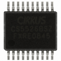
Manufacturer Part Number
CS5526-BSZ
Description
IC ADC 20BIT W/4BIT LATCH 20SSOP
Manufacturer
Cirrus Logic Inc
Datasheet
1.CS5526-BSZ.pdf
(30 pages)
Specifications of CS5526-BSZ
Number Of Converters
1
Package / Case
20-SSOP
Number Of Bits
20
Data Interface
Serial
Power Dissipation (max)
12.7mW
Voltage Supply Source
Analog and Digital
Operating Temperature
-40°C ~ 85°C
Mounting Type
Surface Mount
Number Of Adc Inputs
1
Architecture
Delta-Sigma
Conversion Rate
3.76 SPs to 616 SPs
Resolution
20 bit
Input Type
Voltage
Interface Type
Serial (3-Wire)
Voltage Reference
2.5 V
Supply Voltage (max)
5 V
Supply Voltage (min)
25 mV
Maximum Power Dissipation
500 mW
Maximum Operating Temperature
+ 85 C
Mounting Style
SMD/SMT
Input Voltage
25 mV to 5 V
Minimum Operating Temperature
- 40 C
Lead Free Status / RoHS Status
Lead free / RoHS Compliant
For Use With
598-1014 - EVAL BOARD FOR CS5526
Lead Free Status / Rohs Status
Lead free / RoHS Compliant
Other names
598-1108-5
Available stocks
Company
Part Number
Manufacturer
Quantity
Price
Company:

Part Number:
CS5526-BSZ
Manufacturer:
CIRRUS
Quantity:
1 000
Part Number:
CS5526-BSZ
Manufacturer:
CIRRUS
Quantity:
20 000


ANALOG CHARACTERISTICS
NBV = -2.1 V, FCLK = 32.768 kHz, OWR (Output Word Rate) = 15 Sps, Bipolar Mode, Input Range = ±100 mV;
See Notes 1 and 2.)
Notes: 1. Applies after system calibration at any temperature within -40 °C ~ +85 °C.
RMS NOISE
Notes: 6. Wideband noise aliased into the baseband. Referred to the input. Typical values shown for 25 °C.
2
Accuracy
Linearity Error
No Missing Codes
Bipolar Offset
Unipolar Offset
Offset Drift
Bipolar Gain Error
Unipolar Gain Error
Gain Drift
Voltage Reference Input
Range
Common Mode Rejection
Input Capacitance
CVF Current
123.2 (Note 8)
168.9 (Note 8)
202.3 (Note 8)
Output Rate
(Sps)
3.76
7.51
15.0
30.1
60.0
2. Specifications guaranteed by design, characterization, and/or test.
3. Specification applies to the device only and does not include any effects by external parasitic
4. Drift over specified temperature range after calibration at power-up at 25 °C.
5. See the section of the data sheet which discusses input models on page 15.
7. For Peak-to-Peak Noise multiply by 6.6 for all ranges and output rates.
8. For input ranges <100 mV and output word rates >60 Sps, 32.768 kHz chopping frequency is used.
thermocouples. LSB = LSB
-3 dB Filter
Frequency
(Notes 6 and 7)
Parameter
103.6
141.3
169.2
3.27
6.55
12.7
25.4
50.4
(VREF+) - (VREF-)
dc
50, 60 Hz
Specifications are subject to change without notice.
110 nV
170 nV
250 nV
500 nV
25 mV
2.0 µV
(Notes 3 and 4)
90 nV
10 µV
30 µV
16
(Note 3)
(Note 3)
(Note 4)
(Note 5)
for the CS5525, and LSB
(T
20.0 µV
130 nV
200 nV
300 nV
55 mV
1.0 µV
4.0 µV
A
90 nV
55 µV
= 25 °C; VA+, VD+ = 5 V ±5%; VREF+ = 2.5 V, VREF- = AGND,
Input Range, (Bipolar/Unipolar Mode)
Min
16
1
-
-
-
-
-
-
-
-
-
-
-
CS5525
±0.0015 ±0.003
100 mV
130 nV
190 nV
250 nV
500 nV
105 µV
1.5 µV
8.0 µV
Typ
±16
130
110
30 µV
2.5
0.6
20
±1
±2
±8
16
1
-
20
for the CS5526.
Max
±31
±62
3.0
±2
±4
3
-
-
-
-
-
-
340 µV
1.1 mV
1.0 µV
1.5 µV
2.0 µV
4.0 µV
15 µV
72 µV
1 V
Min
20
1
-
-
-
-
-
-
-
-
-
-
-
CS5525 CS5526
CS5526
±0.0007 ±0.0015
Typ
130
±16
±32
±16
110
190 µV
900 µV
2.4 mV
2.5
0.6
2.0 µV
3.0 µV
5.0 µV
20
±8
16
10 µV
45 µV
2.5 V
1
-
Max
±32
±64
±31
±62
3.0
3
-
-
-
-
-
-
350 µV
2.0 mV
5.3 mV
4.0 µV
10 µV
15 µV
85 µV
DS202F5
7 µV
5 V
ppm/°C
nV/°C
%FS
µA/V
Unit
LSB
LSB
ppm
ppm
Bits
dB
dB
pF
V
Related parts for CS5526-BSZ
Image
Part Number
Description
Manufacturer
Datasheet
Request
R

Part Number:
Description:
IC 20-Bit Delta Sigma Multi-Range ADC
Manufacturer:
Cirrus Logic Inc
Datasheet:

Part Number:
Description:
Development Kit
Manufacturer:
Cirrus Logic Inc
Datasheet:
Part Number:
Description:
Development Kit
Manufacturer:
Cirrus Logic Inc
Datasheet:


Part Number:
Description:
High-efficiency PFC + Fluorescent Lamp Driver Reference Design
Manufacturer:
Cirrus Logic Inc
Datasheet:
Part Number:
Description:
Development Kit
Manufacturer:
Cirrus Logic Inc
Datasheet:
Part Number:
Description:
Development Kit
Manufacturer:
Cirrus Logic Inc
Datasheet:

Part Number:
Description:
Development Kit
Manufacturer:
Cirrus Logic Inc
Datasheet:
Part Number:
Description:
Development Kit
Manufacturer:
Cirrus Logic Inc
Datasheet:
Part Number:
Description:
Development Kit
Manufacturer:
Cirrus Logic Inc
Datasheet:
Part Number:
Description:
Development Kit
Manufacturer:
Cirrus Logic Inc
Datasheet:

Part Number:
Description:
Ref Bd For Speakerbar MSA & DSP Products
Manufacturer:
Cirrus Logic Inc