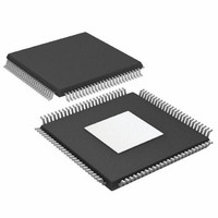
AD9430BSVZ-210 Analog Devices Inc, AD9430BSVZ-210 Datasheet - Page 29

AD9430BSVZ-210
Manufacturer Part Number
AD9430BSVZ-210
Description
IC ADC 12BIT 210MSPS 3.3V100TQFP
Manufacturer
Analog Devices Inc
Datasheet
1.AD9430BSVZ-210.pdf
(44 pages)
Specifications of AD9430BSVZ-210
Data Interface
Parallel
Number Of Bits
12
Sampling Rate (per Second)
210M
Number Of Converters
1
Power Dissipation (max)
1.7mW
Voltage Supply Source
Single Supply
Operating Temperature
-40°C ~ 85°C
Mounting Type
Surface Mount
Package / Case
100-TQFP Exposed Pad
Resolution (bits)
12bit
Sampling Rate
210MSPS
Input Channel Type
Differential
Supply Voltage Range - Digital
3V To 3.6V
Supply Current
390mA
Lead Free Status / RoHS Status
Lead free / RoHS Compliant
Available stocks
Company
Part Number
Manufacturer
Quantity
Price
Company:
Part Number:
AD9430BSVZ-210
Manufacturer:
AD
Quantity:
2 197
Part Number:
AD9430BSVZ-210
Manufacturer:
ADI/亚德诺
Quantity:
20 000
CMOS DATA OUTPUTS
The ADC CMOS digital outputs are latched on the board by
four LVT574s; the latch outputs are available at the two 40-pin
connectors at Pin 11 through Pin 33 on P23 (Channel A) and
Pin 11 through Pin 33 on P3 (Channel B). The latch output
clocks (data ready) are available at Pin 37 on P23 (Channel A)
and Pin 37 on P3 (Channel B). The data-ready clocks can be
inverted at the timing controls section if needed.
CRYSTAL OSCILLATOR
An optional crystal oscillator can be placed on the board to
serve as a clock source for the PCB. Power to the oscillator is
through the VCLK pin at the power connector (also called
VCLK/V_XTAL). If an oscillator is used, ensure proper
termination for best results. The board has been tested with a
Valpey Fisher VF561 and a Vectron JN00158-163.84. Test
results for the VF561 are shown in Figure 56.
–100
1
2
–10
–20
–30
–40
–50
–60
–70
–80
–90
CH1
0
Figure 55. Data Output and Clock @ 80-Pin Connector
0
Figure 56. FFT—Using VF561 Crystal as Clock Source
ENCODE 163.84MHz
ANALOG 65.02MHz
SNR 63.93dB
SINAD 63.87dB
FUND –0.45dBFS
2ND –85.62dBc
3RD –91.31dBc
4TH –90.54dBc
5TH –90.56dBc
6TH –91.12dBc
THD –82.21dBc
SFDR 83.93dBc
SAMPLES 8k
NOISEFLR –100.44dBFS
WORSTSP –83.93dBc
2.00V
20
CH2
2.00V
MHz
40
M 5.00ns
∆: 4.6ns
C1 FREQ
84.65608MHz
60
CH2
80
Rev. E | Page 29 of 44
OPTIONAL AMPLIFIER
The evaluation board as shipped uses a wideband RF
transformer in its analog path. A user can modify the board to
use the AD8351 op amp for ac- or dc-coupled applications
(see Figure 59 and Figure 60). Figure 60 shows the AD8351 in
an ac-coupled topology, while Figure 57 shows the AD8351 in
a dc-coupled application. Optimum performance is obtained
with the AD8351 ac coupled.
SOURCE
SINGLE-
ENDED
50
50
R1
Figure 57. Using the AD8351 on the AD9430 PCB
25
100nF
100nF
R
INLO
G
INHI
R
AD8351
F
VOCM
OPHI
100nF
OPLO
25
25
2.8V
5pF
AD9430
AIN+
AIN–
AD9430
DIGITAL
OUT


