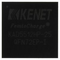
KAD5512HP-25Q72 Intersil, KAD5512HP-25Q72 Datasheet - Page 25

KAD5512HP-25Q72
Manufacturer Part Number
KAD5512HP-25Q72
Description
IC ADC 12BIT 250MSPS SGL 72-QFN
Manufacturer
Intersil
Series
FemtoCharge™r
Datasheet
1.KAD5512HP-25Q72.pdf
(34 pages)
Specifications of KAD5512HP-25Q72
Number Of Bits
12
Sampling Rate (per Second)
250M
Data Interface
Serial, SPI™
Number Of Converters
1
Power Dissipation (max)
463mW
Voltage Supply Source
Single Supply
Operating Temperature
-40°C ~ 85°C
Mounting Type
Surface Mount
Package / Case
72-VFQFN Exposed Pad
For Use With
KDC5512H-Q48EVAL - DAUGHTER CARD FOR KAD5512KDC5512HEVAL - DAUGHTER CARD FOR KAD5512
Lead Free Status / RoHS Status
Lead free / RoHS Compliant
register is read from without properly setting
device_index_A.
ADDRESS 0X20: OFFSET_COARSE
ADDRESS 0X21: OFFSET_FINE
The input offset of each ADC core can be adjusted in fine
and coarse steps. Both adjustments are made via an 8-bit
word as detailed in Table 7.
The default value of each register will be the result of the
self-calibration after initial power-up. If a register is to be
incremented or decremented, the user should first read the
register value then write the incremented or decremented
value back to the same register.
ADDRESS 0X22: GAIN_COARSE
ADDRESS 0X23: GAIN_MEDIUM
ADDRESS 0X24: GAIN_FINE
Gain of the ADC core can be adjusted in coarse, medium
and fine steps. Coarse gain is a 4-bit adjustment while
medium and fine are 8-bit. Multiple Coarse Gain Bits can be
set for a total adjustment range of ± 4.2%. (‘0011’ =~ -4.2%
and ‘1100’ =~ +4.2%) It is recommended to use one of the
coarse gain settings (-4.2%, -2.8%, -1.4%, 0, 1.4%, 2.8%,
4.2%) and fine-tune the gain using the registers at 23h and
24h.
The default value of each register will be the result of the
self-calibration after initial power-up. If a register is to be
incremented or decremented, the user should first read the
register value then write the incremented or decremented
value back to the same register.
+Full Scale (0xFF)
Nominal Step Size
–Full Scale (0x00)
Mid–Scale (0x80)
PARAMETER
0x22[3:0]
Steps
Bit3
Bit2
Bit1
Bit0
TABLE 8. COARSE GAIN ADJUSTMENT
TABLE 7. OFFSET ADJUSTMENTS
COARSE OFFSET
+133LSB (+47mV)
1.04LSB (0.37mV)
-133LSB (-47mV)
0.0LSB (0.0mV)
NOMINAL COARSE GAIN ADJUST
0x20[7:0]
255
25
+2.8
+1.4
-2.8
-1.4
(%)
0.04LSB (0.014mV)
+5LSB (+1.75mV)
-5LSB (-1.75mV)
FINE OFFSET
0x21[7:0]
0.0LSB
255
KAD5512HP
SLIP TWICE
SLIP ONCE
ADDRESS 0X25: MODES
Two distinct reduced power modes can be selected. By
default, the tri-level NAPSLP pin can select normal
operation, nap or sleep modes (refer to “Nap/Sleep” on
page 21). This functionality can be overridden and controlled
through the SPI. This is an indexed function when controlled
from the SPI, but a global function when driven from the pin.
This register is not changed by a Soft Reset.
Global Device Configuration/Control
ADDRESS 0X71: PHASE_SLIP
When using the clock divider, it’s not possible to determine
the synchronization of the incoming and divided clock
phases. This is particularly important when multiple ADCs
are used in a time-interleaved system. The phase slip
feature allows the rising edge of the divided clock to be
advanced by one input clock cycle when in CLK/4 mode, as
shown in Figure 39. Execution of a phase_slip command is
accomplished by first writing a ‘0’ to bit 0 at address 71h
followed by writing a ‘1’ to Bit 0 at address 71h (32 sclk
cycles).
FIGURE 39. PHASE SLIP: CLK÷4 MODE, f
+Full Scale (0xFF)
–Full Scale (0x00)
Nominal Step Size
Mid–Scale (0x80)
CLK÷4
CLK÷4
CLK÷4
PARAMETER
CLK
TABLE 9. MEDIUM AND FINE GAIN ADJUSTMENTS
Steps
VALUE
TABLE 10. POWER-DOWN CONTROL
000
001
010
100
MEDIUM GAIN
CLK = CLKP – CLKN
0x23[7:0]
1.00ns
0.016%
0.00%
+2%
256
-2%
POWER-DOWN MODE
Normal Operation
4.00ns
Sleep Mode
Pin Control
Nap Mode
0x25[2:0]
CLOCK
FINE GAIN
0x24[7:0]
0.0016%
-0.20%
0.00%
+0.2%
256
= 1000MHz
October 1, 2009
FN6808.3


