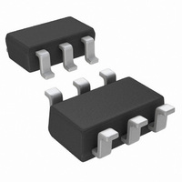
ADC101S021CIMF/NOPB National Semiconductor, ADC101S021CIMF/NOPB Datasheet

ADC101S021CIMF/NOPB
Specifications of ADC101S021CIMF/NOPB
ADC101S021CIMFTR
Related parts for ADC101S021CIMF/NOPB
ADC101S021CIMF/NOPB Summary of contents
Page 1
... Connection Diagram Ordering Information Order Code ADC101S021CISD ADC101S021CISDX ADC101S021CIMF ADC101S021CIMFX ADC101S021EVAL TRI-STATE ® registered trademark of National Semiconductor Corporation. © 2010 National Semiconductor Corporation ADC101S021 Features ■ Specified over a range of sample rates. ■ 6-lead LLP and SOT-23 packages ■ Variable power management ■ ...
Page 2
Block Diagram Pin Descriptions and Equivalent Circuits Pin No. Symbol ANALOG I/O V Analog input. This signal can range from DIGITAL I/O 4 SCLK Digital clock input. This clock directly controls the conversion and readout ...
Page 3
... Absolute Maximum Ratings 2) If Military/Aerospace specified devices are required, please contact the National Semiconductor Sales Office/ Distributors for availability and specifications. Analog Supply Voltage V A Voltage on Any Analog Pin to GND Voltage on Any Digital Pin to GND Input Current at Any Pin (Note 3) Package Input Current ...
Page 4
Symbol Parameter FPBW -3 dB Full Power Bandwidth ANALOG INPUT CHARACTERISTICS V Input Range Leakage Current DCL C Input Capacitance INA DIGITAL INPUT CHARACTERISTICS V Input High Voltage IH V Input Low Voltage IL I Input Current ...
Page 5
Symbol Parameter t (Note 10) QUIET t Aperture Delay AD t Aperture Jitter AJ ADC101S021 Timing Specifications The following specifications apply for ksps to 200 ksps, Boldface limits apply for T SAMPLE Symbol Parameter t Minimum ...
Page 6
Timing Diagrams www.national.com FIGURE 1. Timing Test Circuit FIGURE 2. ADC101S021 Serial Timing Diagram 6 20145308 20145306 ...
Page 7
Specification Definitions ACQUISITION TIME is the time required to acquire the input voltage. That is time required for the hold capacitor to charge up to the input voltage. Acquisition time is measured backwards from the falling edge of ...
Page 8
Typical Performance Characteristics MHz to 4 MHz 100 kHz unless otherwise stated. SCLK IN DNL MHz SCLK DNL MHz SCLK DNL vs. Clock Frequency www.national.com T = +25°C, f ...
Page 9
SNR vs. Clock Frequency 20145363 SFDR vs. Clock Frequency 20145367 Spectral Response 5.25V MHz SCLK 20145369 SINAD vs. Clock Frequency THD vs. Clock Frequency Power Consumption vs. Throughput MHz SCLK 9 ...
Page 10
Applications Information 1.0 ADC101S021 OPERATION The ADC101S021 is a successive-approximation analog-to- digital converter designed around a charge-redistribution dig- ital-to-analog converter core. Simplified schematics of the ADC101S021 in both track and hold modes are shown in Figure 3 and Figure 4, ...
Page 11
... It is possible, however, to 4.0 TYPICAL APPLICATION CIRCUIT A typical application of the ADC is shown in is provided in this example by the National Semiconductor LP2950 low-dropout voltage regulator, available in a variety of fixed and adjustable output voltages. The power supply pin is bypassed with a capacitor network located close to the ADC ...
Page 12
ANALOG INPUTS An equivalent circuit for the ADC's input is shown in 7. Diodes D1 and D2 provide ESD protection for the analog inputs time should the analog input go beyond (V 300 mV) or (GND − ...
Page 13
To exit shutdown mode, bring CS back low. Upon bringing CS low, the ADC will begin powering up (power-up time is specified in the Timing Specifications table). This power-up delay results in the first conversion result being unusable. The second ...
Page 14
Physical Dimensions Order Number ADC101S021CISD or ADC101S021CISDX www.national.com inches (millimeters) unless otherwise noted 6-Lead LLP NS Package Number SDB06A 6-Lead SOT-23 Order Number ADC101S021CIMF, ADC101S021CIMFX NS Package Number MF06A 14 ...
Page 15
Notes 15 www.national.com ...
Page 16
... For more National Semiconductor product information and proven design tools, visit the following Web sites at: www.national.com Products Amplifiers www.national.com/amplifiers Audio www.national.com/audio Clock and Timing www.national.com/timing Data Converters www.national.com/adc Interface www.national.com/interface LVDS www.national.com/lvds Power Management www.national.com/power Switching Regulators www.national.com/switchers LDOs www.national.com/ldo LED Lighting www ...


