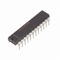
MAX191BCNG+ Maxim Integrated Products, MAX191BCNG+ Datasheet - Page 9

MAX191BCNG+
Manufacturer Part Number
MAX191BCNG+
Description
IC ADC 12BIT 100KSPS W/REF 24DIP
Manufacturer
Maxim Integrated Products
Datasheet
1.MAX191BCWG.pdf
(24 pages)
Specifications of MAX191BCNG+
Number Of Bits
12
Sampling Rate (per Second)
100k
Data Interface
MICROWIRE™, Parallel, QSPI™, Serial, SPI™
Number Of Converters
1
Power Dissipation (max)
1.07W
Voltage Supply Source
Dual ±
Operating Temperature
0°C ~ 70°C
Mounting Type
Through Hole
Package / Case
24-DIP (0.300", 7.62mm)
Number Of Adc Inputs
1
Architecture
SAR
Conversion Rate
100 KSPs
Resolution
12 bit
Input Type
Voltage
Interface Type
Serial
Voltage Reference
Internal 4.096 V or External
Supply Voltage (max)
5 V
Maximum Power Dissipation
1067 mW
Maximum Operating Temperature
+ 70 C
Mounting Style
Through Hole
Minimum Operating Temperature
0 C
Lead Free Status / RoHS Status
Lead free / RoHS Compliant
Figure 4. Equivalent Input Circuit
various interface modes.
The time required for the T/H to acquire an input signal
is a function of how quickly its input capacitance is
charged. If the input signal’s source impedance is high,
the acquisition time lengthens and more time must be
allowed between conversions. Acquisition time is cal-
culated by: t
than 2µs), where R
the input signal, and C
The ADC’s input tracking circuitry has a 1MHz typical
large-signal bandwidth characteristic, and a 30V/µs
slew rate. It is possible to digitize high-speed transients
and measure periodic signals with bandwidths exceed-
ing the ADC’s sample rate of 100ksps by using under-
sampling techniques. Note that if undersampling is
used to measure high-frequency signals, special care
must be taken to avoid aliasing errors. Without ade-
quate input bandpass filtering, out-of-band signals and
noise may be aliased into the measurement band.
Internal protection diodes, which clamp the analog input
to V
(V
However, for accurate conversions near full scale, AIN+
should not exceed the power supplies by more than
50mV because ADC accuracy is affected when the pro-
C
DD
AIN +
PACKAGE
AIN -
DD
5pF
+ 0.3V) with no risk of damage to the ADC.
and V
TRACK
SS
ACQ
, allow AIN+ to swing from (V
HOLD
with Internal Reference and Power-Down
= 10(R
_______________________________________________________________________________________
IN
= 2kΩ, R
HOLD
12-BIT DAC
C
S
C
SWITCH
10pF
32pF
HOLD
+ R
= 32pF (see Figure 4).
IN
S
= source impedance of
)C
HOLD
R
IN
Input Bandwidth
HOLD
Input Protection
Low-Power, 12-Bit Sampling ADC
COMPARATOR
(but never less
SS
- 0.3V) to
tection diodes are even slightly forward biased.
In parallel mode, the ADC is controlled by the CS, RD,
and HBEN inputs, as shown in Figure 6. The T/H
enters hold mode and a conversion starts at the falling
edge of CS and RD while HBEN (not shown) is low.
BUSY goes low as soon as the conversion starts. On
the falling edge of the 13th input clock pulse after the
conversion starts, BUSY goes high and the conversion
result is latched into three-state output buffers. In seri-
al mode, the falling edge of CS initiates a conversion,
and the T/H enters hold mode. Data is shifted out seri-
ally as the conversion proceeds (Figure 10). See the
Parallel Digital-Interface Mode and Serial-Interface
Mode sections for details.
Figure 5 shows the MAX191 clock circuitry. The ADC
includes internal circuitry to generate a clock with an
external capacitor. As indicated in the Typical
Operating Characteristics , a 120pF capacitor con-
nected between the CLK and DGND pins generates
a 1MHz nominal clock frequency (Figure 5).
Alternatively, an external clock (between 100kHz and
1.6MHz) can be applied to CLK. When using an exter-
nal clock source, acceptable clock duty cycles are
Figure 5. Internal Clock Circuit
C
NOTE: C
EXT
EXT
= 120pF GENERATES 1MHz NOMINAL CLOCK
CLK
DGND
Internal/External Clock
Starting a Conversion
MAX191
Digital Interface
+1.6V
CLOCK
9


