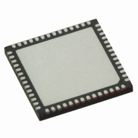
MAX11044ETN+ Maxim Integrated Products, MAX11044ETN+ Datasheet - Page 20

MAX11044ETN+
Manufacturer Part Number
MAX11044ETN+
Description
ADC 16BIT SAMPLING 4CH 56-TQFN
Manufacturer
Maxim Integrated Products
Datasheet
1.MAX11044ETN.pdf
(27 pages)
Specifications of MAX11044ETN+
Number Of Bits
16
Sampling Rate (per Second)
250k
Data Interface
Parallel
Number Of Converters
4
Power Dissipation (max)
2.22W
Voltage Supply Source
Analog and Digital
Operating Temperature
-40°C ~ 85°C
Mounting Type
Surface Mount
Package / Case
56-WQFN Exposed Pad, 56-HWQFN
Number Of Adc Inputs
4
Architecture
SAR
Conversion Rate
250 KSPs
Resolution
16 bit
Input Type
Voltage
Interface Type
Parallel
Snr
92.3 dB
Voltage Reference
Internal 4.096 V
Supply Voltage (max)
5.25 V
Supply Voltage (min)
2.7 V, 4.75 V
Maximum Power Dissipation
2222 mW
Maximum Operating Temperature
+ 85 C
Mounting Style
SMD/SMT
Input Voltage
5 V
Minimum Operating Temperature
- 40 C
Lead Free Status / RoHS Status
Lead free / RoHS Compliant
4-/6-/8-Channel, 16-/14-Bit,
Simultaneous-Sampling ADCs
The MAX11044/MAX11045/MAX11046 and MAX11054/
MAX11055/MAX11056 have a built-in reference buffer
to provide a low-impedance reference source to the
SAR converters. This buffer is used in both internal and
external reference mode. The reference buffer output
feeds five RDC pins. The RDC pins should be all con-
nected together on the PCB. The reference buffer is
Figure 8. Two’s Complement Transfer Function for 16-Bit Devices
Figure 8b. Two’s Complement Transfer Function for 14-Bit Devices
20
______________________________________________________________________________________
1FFF
1FFE
3FFF
3FFE
0001
0000
2001
2000
7FFE
7FFF
FFFF
FFFE
0001
0000
8001
8000
+FS = 8191 x V
V
-FS = -8192 x V
+FS = 32,767 x V
-FS = -32,768 x V
OUTPUT CODE =
V
OUTPUT CODE =
LSB
-FS
LSB
-FS
= (10/4.096) x (V
= (10/4.096) x (V
-8191.5 x V
-32,767.5 x V
LSB
LSB
LSB
LSB
V
V
V
V
LSB
LSB
LSB
IN
INPUT VOLTAGE (LSB)
IN
INPUT VOLTAGE (LSB)
REF
LSB
REF
+ 32,768
+ 8192
/16,384)
/65,536)
FULL-SCALE
FULL-SCALE
TRANSITION
TRANSITION
0
0
+32,766.5 x V
+8190.5 x V
Reference Buffer
LSB
LSB
+FS
+FS
externally compensated and requires at least 10µF on
the RDC node. For best performance, provide a total of
at least 80µF on the RDC outputs.
Figures 8 and 9 show the transfer functions for all the
formats and devices. Code transitions occur halfway
between successive-integer LSB values.
Figure 9. Offset-Binary Transfer Function for 16-Bit Devices
Figure 9b. Offset-Binary Transfer Function for 14-Bit Devices
3FFF
3FFE
2001
2000
1FFF
1FFE
0001
0000
FFFF
FFFE
8001
8000
7FFF
7FFE
0001
0000
+FS = 8191 x V
OUTPUT CODE =
+FS = 32,767 x V
V
-FS = -8192 x V
-FS = -32,768 x V
OUTPUT CODE =
V
-FS
-FS
LSB
LSB
= (10/4.096) x (V
= (10/4.096) x (V
-32,767.5 x V
-8191.5 x V
LSB
LSB
LSB
LSB
V
V
V
V
LSB
LSB
LSB
IN
INPUT VOLTAGE (LSB)
IN
INPUT VOLTAGE (LSB)
LSB
REF
REF
/16,384)
/65,536)
FULL-SCALE
FULL-SCALE
TRANSITION
TRANSITION
0
0
Transfer Functions
+32,766.5 x V
+8190.5 x V
LSB
LSB
+FS
+FS


