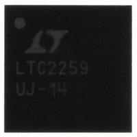
LTC2259CUJ-14#PBF Linear Technology, LTC2259CUJ-14#PBF Datasheet - Page 23

LTC2259CUJ-14#PBF
Manufacturer Part Number
LTC2259CUJ-14#PBF
Description
IC ADC 14-BIT 80MSPS 40-QFN
Manufacturer
Linear Technology
Datasheet
1.LTC2259IUJ-14PBF.pdf
(32 pages)
Specifications of LTC2259CUJ-14#PBF
Number Of Bits
14
Sampling Rate (per Second)
80M
Data Interface
Serial, Parallel
Number Of Converters
1
Power Dissipation (max)
105mW
Voltage Supply Source
Single Supply
Operating Temperature
0°C ~ 70°C
Mounting Type
Surface Mount
Package / Case
40-WFQFN Exposed Pad
Lead Free Status / RoHS Status
Lead free / RoHS Compliant
Available stocks
Company
Part Number
Manufacturer
Quantity
Price
APPLICATIONS INFORMATION
Digital Output Randomizer
Interference from the A/D digital outputs is sometimes
unavoidable. Digital interference may be from capacitive or
inductive coupling or coupling through the ground plane.
Even a tiny coupling factor can cause unwanted tones
in the ADC output spectrum. By randomizing the digital
output before it is transmitted off chip, these unwanted
tones can be randomized which reduces the unwanted
tone amplitude.
The digital output is randomized by applying an exclusive-
OR logic operation between the LSB and all other data
output bits. To decode, the reverse operation is applied—an
exclusive-OR operation is applied between the LSB and
all other bits. The LSB, OF and CLKOUT outputs are not
affected. The output randomizer is enabled by serially
programming mode control register A4.
Figure 15. Functional Equivalent of Digital Output Randomizer
D0
RANDOMIZER
ON
CLKOUT
D13
D12
OF
D2
D1
•
•
•
116114 F15
CLKOUT
OF
D13/D0
D12/D0
D2/D0
D1/D0
D0
Alternate Bit Polarity
Another feature that reduces digital feedback on the circuit
board is the alternate bit polarity mode. When this mode
is enabled, all of the odd bits (D1, D3, D5, D7, D9, D11,
D13) are inverted before the output buffers. The even bits
(D0, D2, D4, D6, D8, D10, D12), OF and CLKOUT are not
affected. This can reduce digital currents in the circuit
board ground plane and reduce digital noise, particularly
for very small analog input signals.
When there is a very small signal at the input of the A/D
that is centered around mid-scale, the digital outputs toggle
between mostly 1s and mostly 0s. This simultaneous
switching of most of the bits will cause large currents in
the ground plane. By inverting every other bit, the alter-
nate bit polarity mode makes half of the bits transition
high while half of the bits transition low. To fi rst order,
this cancels current fl ow in the ground plane, reducing
the digital noise.
Figure 16. Unrandomizing a Randomized Digital
Output Signal
LTC2260-14/LTC2259-14
PC BOARD
LTC2261-14
CLKOUT
D13/D0
D12/D0
D2/D0
D1/D0
OF
D0
FPGA
LTC2261-14
•
•
•
D13
D12
D2
D1
D0
116114 F16
23
226114fa


