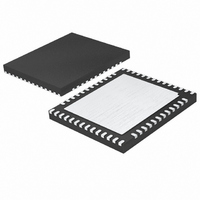
LTC2170IUKG-14#PBF Linear Technology, LTC2170IUKG-14#PBF Datasheet - Page 21

LTC2170IUKG-14#PBF
Manufacturer Part Number
LTC2170IUKG-14#PBF
Description
IC ADC 14BIT SER/PAR 25M 52-QFN
Manufacturer
Linear Technology
Datasheet
1.LTC2172IUKG-14PBF.pdf
(34 pages)
Specifications of LTC2170IUKG-14#PBF
Number Of Bits
14
Sampling Rate (per Second)
25M
Data Interface
Serial, Parallel
Number Of Converters
4
Power Dissipation (max)
243mW
Voltage Supply Source
Analog and Digital
Operating Temperature
-40°C ~ 85°C
Mounting Type
Surface Mount
Package / Case
52-WFQFN Exposed Pad
Number Of Elements
4
Resolution
14Bit
Sample Rate
25MSPS
Input Polarity
Bipolar
Input Type
Voltage
Rated Input Volt
±0.5/±1V
Differential Input
Yes
Power Supply Requirement
Single
Single Supply Voltage (typ)
1.8V
Single Supply Voltage (min)
1.7V
Single Supply Voltage (max)
1.9V
Dual Supply Voltage (typ)
Not RequiredV
Dual Supply Voltage (min)
Not RequiredV
Dual Supply Voltage (max)
Not RequiredV
Power Dissipation
243mW
Differential Linearity Error
±0.8LSB
Integral Nonlinearity Error
±2.75LSB
Operating Temp Range
-40C to 85C
Operating Temperature Classification
Industrial
Mounting
Surface Mount
Pin Count
52
Package Type
QFN EP
Input Signal Type
Differential
Lead Free Status / RoHS Status
Lead free / RoHS Compliant
Available stocks
Company
Part Number
Manufacturer
Quantity
Price
APPLICATIONS INFORMATION
Transformer Coupled Circuits
Figure 3 shows the analog input being driven by an RF
transformer with a center-tapped secondary. The center
tap is biased with V
mal DC level. At higher input frequencies a transmission
line balun transformer (Figures 4 to 6) has better balance,
resulting in lower A/D distortion.
ANALOG
INPUT
ANALOG
INPUT
Figure 4. Recommended Front-End Circuit for Input
Frequencies from 70MHz to 170MHz
T1: MA/COM MABA-007159-000000
T2: MA/COM MABAES0060
RESISTORS, CAPACITORS ARE 0402 PACKAGE SIZE
0.1μF
0.1μF
T1: MA/COM ETC1-1-13
RESISTORS, CAPACITORS
ARE 0402 PACKAGE SIZE
Figure 6. Recommended Front-End Circuit for Input
Frequencies Above 300MHz
0.1μF
0.1μF
T1
T1
CM
, setting the A/D input at its opti-
T2
25Ω
25Ω
25Ω
25Ω
50Ω
2.7nH
2.7nH
0.1μF
0.1μF
50Ω
0.1μF
V
A
A
CM
IN
IN
0.1μF
4.7pF
+
–
V
A
A
CM
IN
IN
+
–
LTC2172-14
LTC2172-14
217214 F06
217214 F04
ANALOG
Amplifi er Circuits
Figure 7 shows the analog input being driven by a high
speed differential amplifi er. The output of the amplifi er is
AC-coupled to the A/D so the amplifi er’s output common
mode voltage can be optimally set to minimize distor-
tion.
At very high frequencies an RF gain block will often have
lower distortion than a differential amplifi er. If the gain
block is single-ended, then a transformer circuit (Figures
4 to 6) should convert the signal to differential before
driving the A/D.
INPUT
ANALOG
INPUT
T1: MA/COM MABA-007159-000000
T2: COILCRAFT WBC1-1LB
RESISTORS, CAPACITORS ARE 0402 PACKAGE SIZE
Figure 5. Recommended Front-End Circuit for Input
Frequencies from 170MHz to 300MHz
0.1μF
0.1μF
LTC2171-14/LTC2170-14
DIFFERENTIAL
HIGH SPEED
+
–
AMPLIFIER
Figure 7. Front-End Circuit Using a High Speed
Differential Amplifi er
T1
+
–
0.1μF
0.1μF
T2
200Ω
25Ω
25Ω
200Ω
LTC2172-14/
25Ω
25Ω
0.1μF
50Ω
12pF
0.1μF
A
A
V
CM
IN
IN
+
–
0.1μF
1.8pF
V
A
A
CM
IN
IN
LTC2172-14
+
–
LTC2172-14
21
21721014fa
217214 F07
217214 F05


