LTC2170IUKG-12#PBF Linear Technology, LTC2170IUKG-12#PBF Datasheet
LTC2170IUKG-12#PBF
Specifications of LTC2170IUKG-12#PBF
Available stocks


Related parts for LTC2170IUKG-12#PBF


LTC2170IUKG-12#PBF Summary of contents
Page 1
... Software Defi ned Radios n Portable Medical Imaging n Multichannel Data Acquisition n Nondestructive Testing L, LT, LTC, LTM, Linear Technology and the Linear logo are registered trademarks of Linear Technology Corporation. All other trademarks are the property of their respective owners. TYPICAL APPLICATION 1. CHANNEL 1 12-BIT ANALOG ...
Page 2
... LTC2171IUKG-12#PBF LTC2171IUKG-12#TRPBF LTC2170CUKG-12#PBF LTC2170CUKG-12#TRPBF LTC2170IUKG-12#PBF LTC2170IUKG-12#TRPBF Consult LTC Marketing for parts specifi ed with wider operating temperature ranges. *The temperature grade is identifi label on the shipping container. For more information on lead free part marking, go to: For more information on tape and reel specifi cations, go to: ...
Page 3
CONVERTER CHARACTERISTICS temperature range, otherwise specifi cations are at T PARAMETER CONDITIONS Resolution (No Missing Codes) Integral Linearity Error Differential Analog Input (Note 6) Differential Linearity Error Differential Analog Input Offset Error (Note 7) Gain Error Internal Reference External Reference ...
Page 4
LTC2172-12/ LTC2171-12/LTC2170-12 DYNAMIC ACCURACY otherwise specifi cations are 25° SYMBOL PARAMETER CONDITIONS SNR Signal-to-Noise Ratio 5MHz Input 30MHz Input 70MHz Input 140MHz Input SFDR Spurious Free Dynamic Range 5MHz Input 2nd or 3rd Harmonic 30MHz ...
Page 5
DIGITAL INPUTS AND OUTPUTS temperature range, otherwise specifi cations are at T SYMBOL PARAMETER + – ENCODE INPUTS (ENC , ENC ) – Differential Encode Mode (ENC Not Tied to GND) V Differential Input Voltage ID V Common Mode Input ...
Page 6
LTC2172-12/ LTC2171-12/LTC2170-12 POWER REQUIREMENTS range, otherwise specifi cations are SYMBOL PARAMETER CONDITIONS V Analog Supply Voltage (Note 10 Output Supply Voltage (Note 10 Analog Supply Current Sine Wave Input VDD I Digital Supply ...
Page 7
TIMING CHARACTERISTICS range, otherwise specifi cations are SYMBOL PARAMETER CONDITIONS Digital Data Outputs (R = 100Ω Differential, C TERM t Serial Data Bit Period 2-Lanes, 16-Bit Serialization SER 2-Lanes, 14-Bit Serialization 2-Lanes, 12-Bit Serialization 1-Lane, 16-Bit Serialization ...
Page 8
LTC2172-12/ LTC2171-12/LTC2170-12 TIMING DIAGRAMS ANALOG INPUT – ENC + ENC – DCO + DCO – – OUT OUT#A – OUT OUT#B SAMPLE N-6 *D AND D ARE EXTRA NON-DATA BITS FOR COMPLETE SOFTWARE ...
Page 9
TIMING DIAGRAMS ANALOG INPUT – ENC + ENC – DCO + DCO + FR – FR – OUT OUT#A – OUT OUT#B SAMPLE N ANALOG INPUT N t ENCH – ENC + ENC – ...
Page 10
LTC2172-12/ LTC2171-12/LTC2170-12 TIMING DIAGRAMS t AP ANALOG INPUT N – ENC + ENC – DCO + DCO – – OUT OUT#A SAMPLE N-6 + – OUT#B ...
Page 11
TYPICAL PERFORMANCE CHARACTERISTICS LTC2172-12: Integral Nonlinearity (INL) 1.0 0.8 0.6 0.4 0.2 0 –0.2 –0.4 –0.6 –0.8 –1.0 0 2048 3072 1024 OUTPUT CODE 217212 G01 LTC2172-12: 8k Point FFT 30MHz IN –1dBFS, 65Msps 0 –10 –20 –30 ...
Page 12
LTC2172-12/ LTC2171-12/LTC2170-12 TYPICAL PERFORMANCE CHARACTERISTICS LTC2172-12: SFDR vs Input Frequency, –1dBFS, 2V Range, 65Msps 100 150 200 250 300 50 INPUT FREQUENCY (MHz) 217212 G10 LTC2172-12 Sample Rate, VDD 5MHz ...
Page 13
TYPICAL PERFORMANCE CHARACTERISTICS LTC2171-12: 8k Point FFT 29MHz IN –1dBFS, 40Msps 0 –10 –20 –30 –40 –50 –60 –70 –80 –90 –100 –110 –120 FREQUENCY (MHz) 217212 G24 LTC2171-12: 8k Point 2-Tone FFT ...
Page 14
LTC2172-12/ LTC2171-12/LTC2170-12 TYPICAL PERFORMANCE CHARACTERISTICS LTC2171-12: SNR vs SENSE 5MHz, –1dBFS 0.6 0.7 0.8 0.9 1 1.1 1.2 1.3 SENSE PIN (V) 217212 G35 LTC2170-12: 8k Point FFT ...
Page 15
TYPICAL PERFORMANCE CHARACTERISTICS LTC2170-12: SNR vs Input Frequency, –1dBFS, 2V Range, 25Msps 100 150 200 250 300 350 INPUT FREQUENCY (MHz) 217212 G49 LTC2170-12 Sample Rate, VDD 5MHz Sine ...
Page 16
LTC2172-12/ LTC2171-12/LTC2170-12 PIN FUNCTIONS + A (Pin 1): Channel 1 Positive Differential Analog IN1 Input. – A (Pin 2): Channel 1 Negative Differential Analog IN1 Input. V (Pin 3): Common Mode Bias Output, Nominally CM12 Equal to V /2. V ...
Page 17
PIN FUNCTIONS PAR/SER (Pin 47): Programming Mode Selection Pin. Connect to ground to enable serial programming mode. CS, SCK, SDI and SDO become a serial interface that con- trols the A/D operating modes. Connect to V parallel programming mode where ...
Page 18
LTC2172-12/ LTC2171-12/LTC2170-12 FUNCTIONAL BLOCK DIAGRAM 1.8V CHANNEL 1 12-BIT SAMPLE- ANALOG ADC CORE AND-HOLD INPUT CHANNEL 2 SAMPLE- 12-BIT ANALOG AND-HOLD ADC CORE INPUT CHANNEL 3 SAMPLE- 12-BIT ANALOG AND-HOLD ADC CORE INPUT CHANNEL 4 SAMPLE- 12-BIT ANALOG AND-HOLD ADC ...
Page 19
APPLICATIONS INFORMATION CONVERTER OPERATION The LTC2172-12/LTC2171-12/LTC2170-12 are low power, 4-channel, 12-bit, 65Msps/40Msps/25Msps A/D convert- ers that are powered by a single 1.8V supply. The analog inputs should be driven differentially. The encode input can be driven differentially for optimal jitter ...
Page 20
LTC2172-12/ LTC2171-12/LTC2170-12 APPLICATIONS INFORMATION Transformer Coupled Circuits Figure 3 shows the analog input being driven transformer with a center-tapped secondary. The center tap is biased with V , setting the A/D input at its opti- CM mal ...
Page 21
APPLICATIONS INFORMATION Reference The LTC2172-12/LTC2171-12/LTC2170-12 has an internal 1.25V voltage reference. For a 2V input range using the internal reference, connect SENSE to V range using the internal reference, connect SENSE to ground. For a 2V input range with an ...
Page 22
LTC2172-12/ LTC2171-12/LTC2170-12 APPLICATIONS INFORMATION The differential encode mode is recommended for sinu- soidal, PECL, or LVDS encode inputs (Figures 12 and 13). The encode inputs are internally biased to 1.2V through 10k equivalent resistance. The encode inputs can be taken ...
Page 23
APPLICATIONS INFORMATION Table 1. Maximum Sampling Frequency for All Serialization Modes. Note That These Limits Are for the LTC2172-12. The Sampling Frequency for the Slower Speed Grades Cannot Exceed 40MHz (LTC2171-12) or 25MHz (LTC2170-12). SERIALIZATION MODE 2-Lane 16-Bit Serialization 2-Lane ...
Page 24
LTC2172-12/ LTC2171-12/LTC2170-12 APPLICATIONS INFORMATION Digital Output Randomizer Interference from the A/D digital outputs is sometimes unavoidable. Digital interference may be from capacitive or inductive coupling or coupling through the ground plane. Even a tiny coupling factor can cause unwanted tones ...
Page 25
APPLICATIONS INFORMATION Serial Programming Mode To use the serial programming mode, PAR/SER should be tied to ground. The CS, SCK, SDI and SDO pins become a serial interface that program the A/D mode control registers. Data is written to a ...
Page 26
LTC2172-12/ LTC2171-12/LTC2170-12 APPLICATIONS INFORMATION REGISTER A2: OUTPUT MODE REGISTER (ADDRESS 02h ILVDS2 ILVDS1 ILVDS0 Bits 7-5 ILVDS2:ILVDS0 LVDS Output Current Bits 000 = 3.5mA LVDS Output Driver Current 001 = 4.0mA LVDS Output Driver Current 010 = 4.5mA ...
Page 27
APPLICATIONS INFORMATION GROUNDING AND BYPASSING The LTC2172-12 requires a printed circuit board with a clean unbroken ground plane. A multilayer board with an internal ground plane in the fi rst layer beneath the ADC is recommended. Layout for the printed ...
Page 28
LTC2172-12/ LTC2171-12/LTC2170-12 TYPICAL APPLICATIONS Silkscreen Top Inner Layer 2 GND 28 Top Side Inner Layer 3 21721012f ...
Page 29
TYPICAL APPLICATIONS Inner Layer 4 Bottom Side LTC2172-12/ LTC2171-12/LTC2170-12 Inner Layer 5 Power Silkscreen Bottom 21721012f 29 ...
Page 30
LTC2172-12/ LTC2171-12/LTC2170-12 TYPICAL APPLICATIONS C17 1μF A IN1 C29 A IN1 0.1μF A IN2 A IN2 C1 C30 C2 2.2μF 0.1μF 0.1μF C3 0.1μF A IN3 A IN3 C59 0.1μF A IN4 A IN4 30 LTC2172 Schematic SENSE C4 R14 ...
Page 31
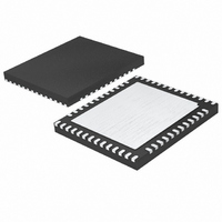
... DRAWING NOT TO SCALE 3. ALL DIMENSIONS ARE IN MILLIMETERS Information furnished by Linear Technology Corporation is believed to be accurate and reliable. However, no responsibility is assumed for its use. Linear Technology Corporation makes no representa- tion that the interconnection of its circuits as described herein will not infringe on existing patent rights. LTC2171-12/LTC2170-12 UKG Package 52-Lead Plastic QFN (7mm × ...
Page 32
... QFN-20 Dual Matched 2nd Order Lowpass Filters with Differential Drivers, Pin-Programmable Gain, 6mm × 3mm DFN-22 Integrated High Speed ADC, Passive Filters and Fixed Gain Differential Amplifi ers www.linear.com ● 21721012f LT 0110 • PRINTED IN USA © LINEAR TECHNOLOGY CORPORATION 2010 ...