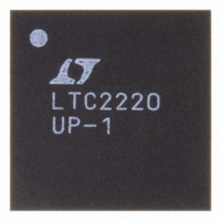
LTC2220CUP-1#PBF Linear Technology, LTC2220CUP-1#PBF Datasheet - Page 14

LTC2220CUP-1#PBF
Manufacturer Part Number
LTC2220CUP-1#PBF
Description
IC ADC 12BIT 185MSPS 64-QFN
Manufacturer
Linear Technology
Datasheet
1.LTC2220CUPPBF.pdf
(32 pages)
Specifications of LTC2220CUP-1#PBF
Number Of Bits
12
Sampling Rate (per Second)
185M
Data Interface
Parallel
Number Of Converters
1
Power Dissipation (max)
1.18W
Voltage Supply Source
Single Supply
Operating Temperature
0°C ~ 70°C
Mounting Type
Surface Mount
Package / Case
64-WFQFN, Exposed Pad
Lead Free Status / RoHS Status
Lead free / RoHS Compliant
Available stocks
Company
Part Number
Manufacturer
Quantity
Price
LTC2220/LTC2221
PI FU CTIO S
MODE (Pin 58): Output Format and Clock Duty Cycle
Stabilizer Selection Pin. Connecting MODE to 0V selects
offset binary output format and turns the clock duty cycle
stabilizer off. Connecting MODE to 1/3V
binary output format and turns the clock duty cycle stabi-
lizer on. Connecting MODE to 2/3V
ment output format and turns the clock duty cycle stabi-
lizer on. Connecting MODE to V
output format and turns the clock duty cycle stabilizer off.
SENSE (Pin 59): Reference Programming Pin. Connecting
SENSE to V
14
U
U
CM
selects the internal reference and a ±0.5V
U
DD
selects 2’s complement
DD
selects 2’s comple-
DD
selects offset
input range. Connecting SENSE to V
reference and a ±1V input range. An external reference
greater than 0.5V and less than 1V applied to SENSE
selects an input range of ±V
input range.
V
Bypass to ground with 2.2µF ceramic chip capacitor.
GND (Exposed Pad) (Pin 65): ADC Power Ground. The
exposed pad on the bottom of the package needs to be
soldered to ground.
CM
(Pin 60): 1.6V Output and Input Common Mode Bias.
SENSE
. ±1V is the largest valid
DD
selects the internal
22201fa


