LTC2220CUP-1#TRPBF Linear Technology, LTC2220CUP-1#TRPBF Datasheet
LTC2220CUP-1#TRPBF
Specifications of LTC2220CUP-1#TRPBF
Available stocks


Related parts for LTC2220CUP-1#TRPBF


LTC2220CUP-1#TRPBF Summary of contents
Page 1
... APPLICATIO S ■ Wireless and Wired Broadband Communication ■ Cable Head-End Systems ■ Power Amplifier Linearization ■ Communications Test Equipment , LTC and LT are registered trademarks of Linear Technology Corporation. All other trademarks are the property of their respective owners. U TYPICAL APPLICATIO 3. REFH FLEXIBLE REFERENCE ...
Page 2
... DD GND 16 EXPOSED PAD (PIN 65) IS GND, MUST BE SOLDERED TO PCB ORDER PART NUMBER LTC2220CUP-1 LTC2220IUP-1 Order Options Tape and Reel: Add #TR Lead Free: Add #PBF Lead Free Tape and Reel: Add #TRPBF Lead Free Part Marking: Consult LTC Marketing for parts specified with wider operating temperature ranges. ...
Page 3
ALOG I PUT The ● denotes the specifications which apply over the full operating temperature range, otherwise specifications are 25°C. (Note 4) A SYMBOL PARAMETER V Analog Input Range ( Analog ...
Page 4
LTC2220 TER AL REFERE CE CHARACTERISTICS PARAMETER V Output Voltage CM V Output Tempco CM V Line Regulation CM V Output Resistance DIGITAL I PUTS A D DIGITAL OUTPUTS full operating temperature range, ...
Page 5
W U POWER REQUIRE E TS range, otherwise specifications are at T SYMBOL PARAMETER V Analog Supply Voltage DD P Shutdown Power SHDN P Nap Mode Power NAP LVDS OUTPUT MODE OV Output Supply Voltage DD I Analog Supply Current ...
Page 6
LTC2220-1 ELECTRICAL CHARACTERISTICS Note 1: Stresses beyond those listed under Absolute Maximum Ratings may cause permanent damage to the device. Exposure to any Absolute Maximum Rating condition for extended periods may affect device reliability and lifetime. Note 2: All voltage ...
Page 7
W U TYPICAL PERFOR A CE CHARACTERISTICS LTC2220-1: SFDR (HD2 and HD3) vs Input Frequency, –1dB, 1V Range, LVDS Mode 100 200 300 0 100 400 500 600 INPUT FREQUENCY (MHz) 2220 G07 LTC2220-1: ...
Page 8
LTC2220 TYPICAL PERFOR A CE CHARACTERISTICS LTC2220-1: 8192 Point FFT 5MHz, –1dB, 2V Range, IN LVDS Mode 0 –20 –40 –60 –80 –100 –120 FREQUENCY (MHz) ...
Page 9
CTIO S (CMOS Mode (Pins 1, 2): Positive Differential Analog Input. IN – A (Pins 3, 4): Negative Differential Analog Input. IN REFHA (Pins 5, 6): ADC High Reference. Bypass to Pins 7, ...
Page 10
LTC2220 CTIO S (LVDS Mode) + AIN (Pins 1, 2): Positive Differential Analog Input. – AIN (Pins 3, 4): Negative Differential Analog Input. REFHA (Pins 5, 6): ADC High Reference. Bypass to Pins 7, 8 ...
Page 11
U U FUNCTIONAL BLOCK DIAGRA + A IN INPUT FIRST PIPELINED S/H ADC STAGE – 1.6V CM REFERENCE 2.2µF RANGE SELECT REF SENSE BUF W SECOND PIPELINED THIRD PIPELINED ADC STAGE ADC STAGE REFH REFL INTERNAL CLOCK ...
Page 12
LTC2220 DIAGRA S ANALOG N INPUT – ENC + ENC D0-D11, OF – CLOCKOUT + CLOCKOUT ANALOG INPUT – ENC + ENC DA0-DA11, OFA CLOCKOUTB CLOCKOUTA DB0-DB11, OFB 12 LVDS Output Mode Timing All ...
Page 13
DIAGRA S ANALOG INPUT – ENC + ENC DA0-DA11, OFA DB0-DB11, OFB CLOCKOUTB CLOCKOUTA Demultiplexed CMOS Outputs with Simultaneous Update ANALOG INPUT – ENC + ENC DA0-DA11, OFA DB0-DB11, OFB CLOCKOUTB CLOCKOUTA Demultiplexed CMOS ...
Page 14
LTC2220 APPLICATIO S I FOR ATIO DYNAMIC PERFORMANCE Signal-to-Noise Plus Distortion Ratio The signal-to-noise plus distortion ratio [S/(N + D)] is the ratio between the RMS amplitude of the fundamental input frequency and the RMS amplitude of all ...
Page 15
U U APPLICATIO S I FOR ATIO Each pipelined stage shown in Figure 1 contains an ADC, a reconstruction DAC and an interstage residue amplifier. In operation, the ADC quantizes the input to the stage and the quantized value is ...
Page 16
LTC2220 APPLICATIO S I FOR ATIO the 2V range or ±0.25V for the 1V range, around a common mode voltage of 1.6V. The V 60) may be used to provide the common mode bias level. V can be ...
Page 17
U U APPLICATIO S I FOR ATIO + – The A and A inputs each have two pins to reduce package inductance. The two A IN should be shorted together. For input frequencies above 100MHz the input ...
Page 18
LTC2220 APPLICATIO S I FOR ATIO Other voltage ranges in between the pin selectable ranges can be programmed with two external resistors as shown in Figure 10. An external reference can be used by applying its output directly ...
Page 19
U U APPLICATIO S I FOR ATIO duty cycle. If the clock is turned off for a long period of time, the duty cycle stabilizer circuit will require one hundred clock cycles for the PLL to lock onto the input ...
Page 20
LTC2220 APPLICATIO S I FOR ATIO As with all high speed/high resolution converters, the digital output loading can affect the performance. The digital outputs of the LTC2220-1 should drive a minimal capacitive load to avoid possible interaction between ...
Page 21
U U APPLICATIO S I FOR ATIO Output Driver Power Separate output power and ground pins allow the output drivers to be isolated from the analog circuitry. The power supply for the digital output buffers the same power ...
Page 22
LTC2220 APPLICATIO S I FOR ATIO Clock Sources for Undersampling Undersampling raises the bar on the clock source and the higher the input frequency, the greater the sensitivity to clock jitter or phase noise. A clock source that ...
Page 23
U U APPLICATIO S I FOR ATIO W U LTC2220-1 2220_1fa 23 ...
Page 24
LTC2220 APPLICATIO S I FOR ATIO Silkscreen Top 2220_1fa ...
Page 25
U U APPLICATIO S I FOR ATIO W U Layer 1 Component Side Layer 2 GND Plane LTC2220-1 2220_1fa 25 ...
Page 26
LTC2220 APPLICATIO S I FOR ATIO Layer 3 Power Plane Layer 4 Bottom Side 2220_1fa ...
Page 27
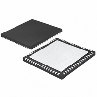
... SHADED AREA IS ONLY A REFERENCE FOR PIN 1 LOCATION ON THE TOP AND BOTTOM OF PACKAGE 6. DRAWING NOT TO SCALE Information furnished by Linear Technology Corporation is believed to be accurate and reliable. However, no responsibility is assumed for its use. Linear Technology Corporation makes no represen- tation that the interconnection of its circuits as described herein will not infringe on existing patent rights Package 64-Lead Plastic QFN (9mm × ...
Page 28
... BW, 47dB OIP3, Digital Gain Control 10.5dB to 33dB in 1.5dB/Step High IIP3: 20dBm at 1.9GHz, Integrated LO Quadrature Generator 4.5V to 5.25V Supply, 25dBm IIP3 at 900MHz 12.5dB, 50Ω Single Ended RF and LO Ports www.linear.com ● 2220_1fa LT 0106 REV A • PRINTED IN USA © LINEAR TECHNOLOGY CORPORATION 2005 ...