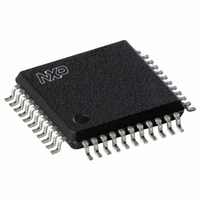
ADC1006S055H/C1,55 NXP Semiconductors, ADC1006S055H/C1,55 Datasheet - Page 11

ADC1006S055H/C1,55
Manufacturer Part Number
ADC1006S055H/C1,55
Description
IC ADC 10BIT PAR 55MHZ 44-QFP
Manufacturer
NXP Semiconductors
Datasheet
1.ADC1006S055HC155.pdf
(31 pages)
Specifications of ADC1006S055H/C1,55
Number Of Bits
10
Sampling Rate (per Second)
55M
Data Interface
Parallel
Number Of Converters
1
Power Dissipation (max)
660mW
Voltage Supply Source
Analog and Digital
Operating Temperature
-40°C ~ 85°C
Mounting Type
Surface Mount
Package / Case
44-MQFP, 44-PQFP
Lead Free Status / RoHS Status
Lead free / RoHS Compliant
Other names
568-4434-5
935286763551
ADC1006S055H/C1
ADC1006S055H/C1-S
ADC1006S055H/C1-S
935286763551
ADC1006S055H/C1
ADC1006S055H/C1-S
ADC1006S055H/C1-S
Available stocks
Company
Part Number
Manufacturer
Quantity
Price
Company:
Part Number:
ADC1006S055H/C1,55
Manufacturer:
IDT, Integrated Device Technology Inc
Quantity:
10 000
NXP Semiconductors
Table 6.
V
V
V
and V
[1]
[2]
[3]
[4]
[5]
[6]
[7]
[8]
[9]
ADC1006S055_070_2
Product data sheet
Symbol
Timing (C
t
t
t
3-state output delay times; see
t
t
t
t
d(s)
h(o)
d(o)
dZH
dZL
dHZ
dLZ
CCA
CCO
I(IN)(p-p)
D = guaranteed by design; C = guaranteed by characterization; I = 100 % industrially tested.
The circuit has two clock inputs: CLK and CLKN. There are 5 modes of operation:
a) PECL mode 1: (DC level vary 1 : 1 with V
b) PECL mode 2: (DC level vary 1 : 1 with V
c) PECL mode 3: (DC level vary 1 : 1 with V
d) Differential AC driving mode 4: When driving the CLK input directly and with any AC signal of minimum 1 V (p-p) and with a DC level
e) TTL mode 1: CLK input is at TTL level and sampling is taken on the falling edge of the clock input signal. In that case CLKN pin has
The ADC input range can be adjusted with an external reference connected to VREF pin. This voltage has to be referenced to V
see
The 3 dB analog bandwidth is determined by the 3 dB reduction in the reconstructed output, the input being a full-scale sine wave.
Total Harmonic Distortion (THD) is obtained with the addition of the first five harmonics:
where
Signal-to-noise ratio (S/N) takes into account all harmonics above five and noise up to Nyquist frequency; see
Effective number of bits are obtained via a Fast Fourier Transform (FFT). The calculation takes into account all harmonics and noise up
to half of the clock frequency (Nyquist frequency). Conversion to SIgnal-to_Noise_Distortion ratio (SINAD) is given by
SINAD = ENOB
Intermodulation measured relative to either tone with analog input frequencies of 20 MHz and 20.1 MHz. The two input signals have the
same amplitude and the total amplitude of both signals provides full-scale to the converter ( 6 dB below full scale for each input signal).
IMD3 is the ratio of the RMS value of either input tone to the RMS value of the worst case third order intermodulation product.
Output data acquisition: the output data is available after the maximum delay of t
THD
= V2 to V44, V3 to V4 and V41 to V40 = 4.75 V to 5.25 V; V
= V33 to V34 = 3.0 V to 3.6 V; AGND and DGND shorted together; T
CCO
signal. A DC level of 3.65 V has to be applied on CLKN decoupled to GND via a 100 nF capacitor.
signal. A DC level of 3.65 V has to be applied on CLK decoupled to GND via a 100 nF capacitor.
of 2.5 V, the sampling takes place at the falling edge of the clock signal. When driving the CLKN input with the same signal, sampling
takes place at the rising edge of the clock signal. It is recommended to decouple the CLKN or CLK input to DGND via a 100 nF
capacitor.
to be connected to the ground.
Figure
=
= 3.3 V, T
V
L
1H
Characteristics
I(INN)(p-p)
20 log
= 10 pF)
Parameter
sampling delay time
output hold time
output delay time
float to active HIGH
delay time
float to active LOW
delay time
active HIGH to float
delay time
active LOW to float
delay time
is the fundamental harmonic referenced at 0 dB for a full-scale sine wave input; see
12.
amb
--------------------------------------------------------------------------------------------------------------------------------------- -
6.02 + 1.76 dB; see
= 1.9 V; V
[9]
2H
= 25 C and C
2
+
…continued
VREF
3H
Figure 4
Conditions
= V
2
L
+
Figure
CCA3
= 10 pF; unless otherwise specified.
a
1H
4H
CCD
CCD
CCD
2
5.
1.75 V; V
2
) CLKN input is at PECL level and sampling is taken on the rising edge of the clock input
) CLK input is at PECL level and sampling is taken on the falling edge of the clock input
) CLK and CLKN inputs are at differential PECL levels.
+
Rev. 02 — 12 August 2008
2
I(cm)
+
= V
6H
CCA3
2
Test
C
C
C
C
C
C
C
CCD
= V37 to V38 and V15 to V17 = 4.75 V to 5.25 V;
[1]
1.6 V; typical values measured at V
Single 10 bits ADC, up to 55 MHz or 70 MHz
Min
-
4
-
-
-
-
-
amb
d(o)
= 40 C to +85 C;
; see
ADC1006S055/070
Figure
Typ
0.25
6.4
9.0
5.1
7.0
9.7
9.5
Figure
3.
6.
Max
1
-
13
9.0
11
14
13
Figure
© NXP B.V. 2008. All rights reserved.
CCA
8.
= V
CCD
Unit
ns
ns
ns
ns
ns
ns
ns
11 of 31
CCA
= 5 V
;


