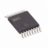
MX7705EUE+ Maxim Integrated Products, MX7705EUE+ Datasheet - Page 18

MX7705EUE+
Manufacturer Part Number
MX7705EUE+
Description
IC ADC 16BIT 2CH 16-TSSOP
Manufacturer
Maxim Integrated Products
Datasheet
1.MX7705EPE.pdf
(33 pages)
Specifications of MX7705EUE+
Number Of Bits
16
Sampling Rate (per Second)
500
Data Interface
MICROWIRE™, QSPI™, Serial, SPI™
Number Of Converters
1
Power Dissipation (max)
755mW
Voltage Supply Source
Single Supply
Operating Temperature
-40°C ~ 85°C
Mounting Type
Surface Mount
Package / Case
16-TSSOP
Lead Free Status / RoHS Status
Lead free / RoHS Compliant
To minimize gain errors in unbuffered mode, select a
source impedance less than the maximum values
shown in Figures 2 and 3. These are the maximum
external resistance/capacitance combinations allowed
before gain errors greater than 1 LSB are introduced in
unbuffered mode.
Enable the internal input buffer for a high source imped-
ance. This isolates the inputs from the sampling capaci-
tor and reduces the sampling-related gain error. When
using the internal buffer, limit the absolute input voltage
range to (V
common-mode voltage range properly to minimize lin-
earity errors.
In unbuffered mode, the absolute analog input voltage
range is from (GND - 30mV) to (V
Electrical Characteristics ). In buffered mode, the ana-
log input voltage range is reduced to (GND + 50mV) to
(V
the differential analog input range (V
decreases at higher gains (see the Programmable-Gain
Amplifier and the Unipolar and Bipolar Modes sections).
The MX7705 provides differential inputs, REF+ and REF-,
for an external reference voltage. Connect the external
reference directly across REF+ and REF- to obtain the
differential reference voltage, V
voltage range for V
and V
V
and 1.225V for V
The MX7705 samples REF+ and REF- at f
(CLKDIV = 0) or f
internal 10pF (typ for gain = 1) sampling capacitor in
series with a 7kΩ (typ) switch on-resistance.
A PGA provides selectable levels of gain: 1, 2, 4, 8, 16,
32, 64, and 128. Bits G0, G1, and G2 in the setup reg-
ister control the gain (Table 9). As the gain increases,
the value of the input sampling capacitor, C
increases (Table 5). The dynamic load presented to the
analog inputs increases with clock frequency and gain
in unbuffered mode (see the Input Buffers section and
Figure 1).
16-Bit, Low-Power, 2-Channel,
Sigma-Delta ADC
18
REF
DD
______________________________________________________________________________________
- 1.5V). In both buffered and unbuffered modes,
(V
DD
REF+
. For specified operation, the nominal voltage,
GND
- V
REF-
+ 50mV) to (V
DD
Programmable-Gain Amplifier
CLKIN
= 2.7V to 3.6V.
), is 2.5V for V
REF+
/ 128 (CLKDIV = 1) with an
and V
Input Voltage Range
DD
REF
REF-
DD
- 1.5V). Set gain and
. The common-mode
DD
+ 30mV) (see the
is between GND
= 4.75V to 5.25V
AIN+
Reference
CLKIN
SAMP
- V
, also
AIN-
/ 64
)
Figure 1. Unbuffered Analog Input Structure
Figure 2. Maximum External Resistance vs. Maximum External
Capacitance for Unbuffered Mode (1MHz)
Figure 3. Maximum External Resistance vs. Maximum External
Capacitance for Unbuffered Mode (2.4576MHz)
AIN(+)
AIN(-)
100
100
0.1
0.1
10
10
1
1
1
1
GAIN = 4
R
GAIN = 8 TO 128
GAIN = 4
GAIN = 8 TO 128
SW
EXTERNAL CAPACITANCE (pF)
EXTERNAL CAPACITANCE (pF)
10
10
(7kΩ TYP)
GAIN = 1
GAIN = 1
V
100
100
BIAS
GAIN = 2
GAIN = 2
C
TOTAL
C
TOTAL
IMPEDANCE
1000
1000
(7pF TYP FOR GAIN = 1)
HIGH
= C
SAMP
10,000
10,000
+ C
STRAY


