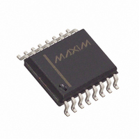
MX7705EWE+ Maxim Integrated Products, MX7705EWE+ Datasheet - Page 25

MX7705EWE+
Manufacturer Part Number
MX7705EWE+
Description
IC ADC 16BIT 2CH 16-SOIC
Manufacturer
Maxim Integrated Products
Datasheet
1.MX7705EPE.pdf
(33 pages)
Specifications of MX7705EWE+
Number Of Bits
16
Sampling Rate (per Second)
500
Data Interface
MICROWIRE™, QSPI™, Serial, SPI™
Number Of Converters
1
Voltage Supply Source
Single Supply
Operating Temperature
-40°C ~ 85°C
Mounting Type
Surface Mount
Package / Case
16-SOIC (0.300", 7.50mm Width)
Lead Free Status / RoHS Status
Lead free / RoHS Compliant
This register is reserved for factory testing of the device.
For proper operation of the MX7705, do not change this
register from its default power-on reset values.
The MX7705 contains one offset register and one gain
register for each input channel. Each register is 24 bits
wide and can be written and read. The offset registers
store the calibration coefficients resulting from a zero-
scale calibration, and the gain registers store the cali-
bration coefficients resulting from a full-scale
calibration. The data stored in these registers are 24-bit
straight binary values representing the offset or gain
errors associated with the selected channel. A 24-bit
read or write operation can be performed on the cali-
bration registers for any selected channel. During a
write operation, 24 bits of data must be written to the
register, or no data is transferred.
Table 12. Clock Register
Table 13. Output Data Rate and Notch Frequency vs. Filter Select and CLKIN Frequency
* These values are given for CLKDIV = 0. External clock frequency, f CLKIN , can be two times the values in this column if CLKDIV = 1.
** The filter -3dB filter cutoff frequency = 0.262 x filter first-notch frequency.
Name
Defaults
FUNCTION
CLKIN FREQUENCY
f
CLKIN
FIRST BIT (MSB)
2.4576
2.4576
2.4576
2.4576
1
1
1
1
(MHz)*
MXID
Offset and Gain-Calibration Registers
1
______________________________________________________________________________________
RESERVED
ZERO
0
ZERO
CLK
0
0
0
0
0
1
1
1
1
DISABLE
CLKOUT
CLKDIS
Test Register
0
FS1
16-Bit, Low-Power, 2-Channel,
0
0
1
1
0
0
1
1
DIVIDER
CLOCK
CLKDIV
FS0
0
1
0
1
0
1
0
1
0
Write to the calibration registers in normal mode only.
After writing to the calibration registers, the devices
implement the new offset and gain-register calibration
coefficients at the beginning of a new acquisition. To
ensure the results are valid, discard the first conversion
result after writing to the calibration registers.
To ensure that a conversion is not made using invalid
calibration data, drive FSYNC high prior to writing to the
calibration registers, and then release FSYNC low to ini-
tiate conversion.
At power-up, the serial-interface, logic, digital-filter, and
modulator circuits are reset. The registers are set to
their default values. The device returns to wait for a
write to the communications register. For accurate
measurements, perform calibration routines after
power-up. Allow time for the external reference and
oscillator to start up before starting calibration. See the
Typical Operating Characteristics for typical external-
oscillator startup times.
OUTPUT DATA RATE
(FIRST NOTCH) (Hz)
SELECT
CLOCK
CLK
1
Sigma-Delta ADC
100
200
250
500
20
25
50
60
FS1
0
FILTER SELECT
-3dB FILTER CUTOFF**
Power-On Reset
131.00
26.20
52.40
13.10
15.70
65.50
(Hz)
5.24
6.55
FS0
1
(LSB)
25


