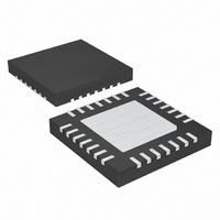
MAX1192ETI+ Maxim Integrated Products, MAX1192ETI+ Datasheet - Page 20

MAX1192ETI+
Manufacturer Part Number
MAX1192ETI+
Description
IC ADC 8BIT 22MSPS DUAL 28-TQFN
Manufacturer
Maxim Integrated Products
Datasheet
1.MAX1192ETI.pdf
(27 pages)
Specifications of MAX1192ETI+
Number Of Bits
8
Sampling Rate (per Second)
22M
Data Interface
Parallel
Number Of Converters
2
Voltage Supply Source
Single Supply
Operating Temperature
-40°C ~ 85°C
Mounting Type
Surface Mount
Package / Case
28-WFQFN Exposed Pad
Number Of Adc Inputs
2
Conversion Rate
22 MSPs
Resolution
8 bit
Input Type
Differential
Interface Type
Parallel
Voltage Reference
Internal 2.048 V or External
Supply Voltage (max)
3.6 V
Supply Voltage (min)
2.7 V
Maximum Power Dissipation
1667 mW
Maximum Operating Temperature
+ 85 C
Mounting Style
SMD/SMT
Minimum Operating Temperature
- 40 C
Lead Free Status / RoHS Status
Lead free / RoHS Compliant
In idle mode, the pipeline ADCs, reference, and clock
distribution circuits are powered, but the outputs are
forced to tri-state. The wake-up time from idle mode is
dominated by the 5ns required for the output drivers to
start from tri-state. When the outputs transition from tri-
state to on, the last converted word is placed on the
digital outputs.
In the normal operating mode, all sections of the
MAX1192 are powered.
Ultra-Low-Power, 22Msps, Dual 8-Bit ADC
Figure 7. DC-Coupled Differential Input Driver
20
V
OPERATIONAL AMPLIFIERS
CHOOSE EITHER OF THE MAX4452/MAX4453/MAX4454 SINGLE/
DUAL/QUAD +3V, 200MHz OP AMPS FOR USE WITH THIS CIRCUIT.
CONNECT THE POSITIVE SUPPLY RAIL (V
0.1μF CAPACITOR TO GROUND.
______________________________________________________________________________________
COM
NEGATIVE SUPPLY RAIL (V
V
SIG
= 1V TO 1.5V
= ±85mV
P-P
EE
R2
300Ω
) TO GROUND. DECOUPLE V
600Ω
600Ω
R3
R1
CC
) TO 3V. CONNECT THE
CC
WITH A
600Ω
600Ω
600Ω
600Ω
R10
R4
R6
R8
600Ω
600Ω
600Ω
600Ω
R11
R7
R9
R5
The circuit of Figure 7 operates from a single 3V supply
and accommodates a wide 0.5V to 1.5V input common-
mode voltage range for the analog interface between
an RF quadrature demodulator (differential, DC-cou-
pled signal source) and a high-speed ADC.
Furthermore, the circuit provides required SINAD and
SFDR to demodulate a wideband (BW = 3.84MHz),
QAM-16 communication link. R
output from the ADC capacitive input to prevent ringing
and oscillation. C
RESISTOR NETWORKS
RESISTOR NETWORKS ENSURE PROPER THERMAL AND TOLERANCE
MATCHING. FOR R1, R2, AND R3 USE A NETWORK SUCH AS VISHAY'S
3R MODEL NUMBER 300192. FOR R4–R11, USE A NETWORK SUCH AS
VISHAY'S 4R MODEL NUMBER 300197.
R
22Ω
R
22Ω
ISO
ISO
Applications Information
IN
filters high-frequency noise.
C
5pF
C
5pF
IN
IN
INA-
COM
INA+
ISO
MAX1192
A
V
V
COM
= 6V/V
isolates the op amp
= V
DD
/2


