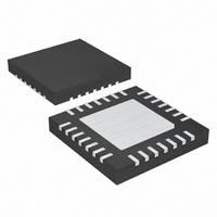
MAX1192ETI+ Maxim Integrated Products, MAX1192ETI+ Datasheet - Page 24

MAX1192ETI+
Manufacturer Part Number
MAX1192ETI+
Description
IC ADC 8BIT 22MSPS DUAL 28-TQFN
Manufacturer
Maxim Integrated Products
Datasheet
1.MAX1192ETI.pdf
(27 pages)
Specifications of MAX1192ETI+
Number Of Bits
8
Sampling Rate (per Second)
22M
Data Interface
Parallel
Number Of Converters
2
Voltage Supply Source
Single Supply
Operating Temperature
-40°C ~ 85°C
Mounting Type
Surface Mount
Package / Case
28-WFQFN Exposed Pad
Number Of Adc Inputs
2
Conversion Rate
22 MSPs
Resolution
8 bit
Input Type
Differential
Interface Type
Parallel
Voltage Reference
Internal 2.048 V or External
Supply Voltage (max)
3.6 V
Supply Voltage (min)
2.7 V
Maximum Power Dissipation
1667 mW
Maximum Operating Temperature
+ 85 C
Mounting Style
SMD/SMT
Minimum Operating Temperature
- 40 C
Lead Free Status / RoHS Status
Lead free / RoHS Compliant
Ultra-Low-Power, 22Msps, Dual 8-Bit ADC
Quadrature amplitude modulation (QAM) is frequently
used in digital communications. Typically found in
spread-spectrum-based systems, a QAM signal repre-
sents a carrier frequency modulated in both amplitude
and phase. At the transmitter, modulating the baseband
signal with quadrature outputs, a local oscillator fol-
lowed by subsequent upconversion can generate the
QAM signal. The result is an in-phase (I) and a quadra-
ture (Q) carrier component, where the Q component is
90° phase shifted with respect to the in-phase compo-
nent. At the receiver, the QAM signal is demodulated
into analog I and Q components.
demodulation process performed in the analog domain
using the MAX1192 dual-matched, 3V, 8-bit ADC and
the MAX2451 quadrature demodulator to recover and
digitize the I and Q baseband signals. Before being dig-
itized by the MAX1192, the mixed-down signal compo-
nents can be filtered by matched analog filters, such as
Nyquist or pulse-shaping filters. The filters remove
unwanted images from the mixing process, thereby
enhancing the overall signal-to-noise (SNR) perfor-
mance and minimizing intersymbol interference.
The MAX1192 requires high-speed board layout design
techniques. Refer to the MAX1193 Evaluation Kit data
sheet for a board layout reference. Locate all bypass
capacitors as close to the device as possible, prefer-
Figure 12. Typical QAM Receiver Application
24
______________________________________________________________________________________
Typical QAM Demodulation Application
Grounding, Bypassing,
and Board Layout
Figure
DOWNCONVERTER
12 displays the
MAX2451
ably on the same side as the ADC, using surface-
mount devices for minimum inductance. Bypass V
GND with a 0.1µF ceramic capacitor in parallel with a
2.2µF bipolar capacitor. Bypass OV
0.1µF ceramic capacitor in parallel with a 2.2µF bipolar
capacitor. Bypass REFP, REFN, and COM each to
GND with a 0.33µF ceramic capacitor.
Multilayer boards with separated ground and power
planes produce the highest level of signal integrity. Use
a split ground plane arranged to match the physical
location of the analog ground (GND) and the digital
output driver ground (OGND) on the ADC’s package.
Connect the MAX1192 exposed backside paddle to
GND. Join the two ground planes at a single point such
that the noisy digital ground currents do not interfere
with the analog ground plane. The ideal location of this
connection can be determined experimentally at a
point along the gap between the two ground planes,
which produces optimum results. Make this connection
with a low-value, surface-mount resistor (1Ω to 5Ω), a
ferrite bead, or a direct short. Alternatively, all ground
pins could share the same ground plane, if the ground
plane is sufficiently isolated from any noisy, digital sys-
tems ground plane (e.g., downstream output buffer or
DSP ground plane).
Route high-speed digital signal traces away from the
sensitive analog traces of either channel. Make sure to
isolate the analog input lines to each respective con-
verter to minimize channel-to-channel crosstalk. Keep
all signal lines short and free of 90° turns.
÷ 8
0°
90°
INA+
INA-
INB+
INB-
MAX1192
DD
A/B
to OGND with a
PROCESSING
POST-
DSP
DD
to


