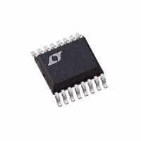
LTC2436-1IGN Linear Technology, LTC2436-1IGN Datasheet - Page 10

LTC2436-1IGN
Manufacturer Part Number
LTC2436-1IGN
Description
IC CONV A/D 16B 2CH DIFF 16SSOP
Manufacturer
Linear Technology
Datasheet
1.LTC2436-1CGN.pdf
(28 pages)
Specifications of LTC2436-1IGN
Number Of Bits
16
Sampling Rate (per Second)
6.8
Data Interface
MICROWIRE™, Serial, SPI™
Number Of Converters
1
Power Dissipation (max)
1mW
Voltage Supply Source
Single Supply
Operating Temperature
-40°C ~ 85°C
Mounting Type
Surface Mount
Package / Case
16-SSOP (0.150", 3.90mm Width)
Lead Free Status / RoHS Status
Contains lead / RoHS non-compliant
Available stocks
Company
Part Number
Manufacturer
Quantity
Price
Company:
Part Number:
LTC2436-1IGN
Manufacturer:
LT
Quantity:
10 000
Part Number:
LTC2436-1IGN#TRPBF
Manufacturer:
LINEAR/凌特
Quantity:
20 000
APPLICATIO S I FOR ATIO
LTC2436-1
Bit 18 (first output bit) is the end of conversion (EOC)
indicator. This bit is available at the SDO pin during the
conversion and sleep states whenever the CS pin is LOW.
This bit is HIGH during the conversion and goes LOW
when the conversion is complete.
Bit 17 (second output bit) is the selected channel indicator.
The bit is LOW for channel 0 and HIGH for channel 1
selected.
Bit 16 (third output bit) is the conversion result sign indi-
cator (SIG). If V
bit is LOW.
Bit 15 (fourth output bit) is the most significant bit (MSB)
of the result. This bit in conjunction with Bit 16 also
provides the underrange or overrange indication. If both
Bit 16 and Bit 15 are HIGH, the differential input voltage is
above +FS. If both Bit 16 and Bit 15 are LOW, the
differential input voltage is below –FS.
The function of these bits is summarized in Table 1.
Table 1. LTC2436-1 Status Bits
Input Range
V
0V V
–0.5 • V
V
Bits 15-0 are the 16-Bit conversion result MSB first.
Bit 0 is the least significant bit (LSB).
Data is shifted out of the SDO pin under control of the serial
clock (SCK), see Figure 3. Whenever CS is HIGH, SDO
10
IN
IN
< – 0.5 • V
0.5 • V
IN
REF
< 0.5 • V
REF
V
REF
IN
REF
< 0V
SDO
SCK
CS
IN
SLEEP
is >0, this bit is HIGH. If V
U
Hi-Z
U
BIT 18
EOC
1
Bit 18
EOC
0
0
0
0
CH0/CH1
W
BIT 17
CH0/CH1
Bit 17
0 or 1
0 or 1
0 or 1
0 or 1
2
BIT 16
IN
SIG
Bit 16 Bit 15
Figure 3. Output Data Timing
U
SIG
is <0, this
3
1
1
0
0
BIT 15
MSB
MSB
1
0
1
0
4
DATA OUTPUT
BIT 14
remains high impedance and any externally generated
SCK clock pulses are ignored by the internal data out shift
register.
In order to shift the conversion result out of the device, CS
must first be driven LOW. EOC is seen at the SDO pin of the
device once CS is pulled LOW. EOC changes real time from
HIGH to LOW at the completion of a conversion. This
signal may be used as an interrupt for an external micro-
controller. Bit 18 (EOC) can be captured on the first rising
edge of SCK. Bit 17 is shifted out of the device on the first
falling edge of SCK. The final data bit (Bit 0) is shifted out
on the falling edge of the 18th SCK and may be latched on
the rising edge of the 19th SCK pulse. On the falling edge
of the 19th SCK pulse, SDO goes HIGH indicating the
initiation of a new conversion cycle. This bit serves as EOC
(Bit 18) for the next conversion cycle. Table 2 summarizes
the output data format.
In order to remain compatible with some SPI
microcontrollers, more than 19 SCK clock pulses may be
applied. As long as these clock edges are complete before
the conversion ends, they will not effect the serial data.
However, switching SCK during a conversion may gener-
ate ground currents in the device leading to extra offset
and noise error sources.
As long as the voltage on the analog input pins is main-
tained within the – 0.3V to (V
operating range, a conversion result is generated for any
differential input voltage V
+FS = 0.5 • V
+FS, the conversion result is clamped to the value corre-
sponding to the +FS + 1LSB. For differential input voltages
5
17
REF
. For differential input voltages greater than
BIT 1
18
LSB
BIT 0
IN
16
CC
19
from –FS = –0.5 • V
+ 0.3V) absolute maximum
CONVERSION
24361 F03
REF
24361f
to


