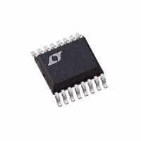
LTC2436-1IGN Linear Technology, LTC2436-1IGN Datasheet - Page 21

LTC2436-1IGN
Manufacturer Part Number
LTC2436-1IGN
Description
IC CONV A/D 16B 2CH DIFF 16SSOP
Manufacturer
Linear Technology
Datasheet
1.LTC2436-1CGN.pdf
(28 pages)
Specifications of LTC2436-1IGN
Number Of Bits
16
Sampling Rate (per Second)
6.8
Data Interface
MICROWIRE™, Serial, SPI™
Number Of Converters
1
Power Dissipation (max)
1mW
Voltage Supply Source
Single Supply
Operating Temperature
-40°C ~ 85°C
Mounting Type
Surface Mount
Package / Case
16-SSOP (0.150", 3.90mm Width)
Lead Free Status / RoHS Status
Contains lead / RoHS non-compliant
Available stocks
Company
Part Number
Manufacturer
Quantity
Price
Company:
Part Number:
LTC2436-1IGN
Manufacturer:
LT
Quantity:
10 000
Part Number:
LTC2436-1IGN#TRPBF
Manufacturer:
LINEAR/凌特
Quantity:
20 000
APPLICATIO S I FOR ATIO
by Figures 14 and 15. For simplicity, two distinct situa-
tions can be considered.
For relatively small values of input capacitance (C
0.01 F), the voltage on the sampling capacitor settles
almost completely and relatively large values for the
source impedance result in only small errors. Such values
for C
performance without significant benefits of signal filtering
and the user is advised to avoid them. Nevertheless, when
small values of C
of input multiplexers, wires, connectors or sensors, the
LTC2436-1 can maintain its accuracy while operating with
relative large values of source resistance as shown in
Figure 15. –FS Error vs R
Figure 17. –FS Error vs R
IN
will deteriorate the converter offset and gain
–12
–16
–20
–1
–2
–3
–4
–8
0
0
1
0 100 200 300 400 500 600 700 800 900 1000
V
REF
REF
IN
IN
F
T
O
V
REF
REF
IN
IN
F
T
CC
A
O
+
–
A
CC
= GND
= 25 C
+
–
+
–
= GND
= 2.5V
= GND
= 25 C
= 5V
+
–
= 1.25V
= 3.75V
= 5V
IN
= 5V
= GND
= 5V
= GND
10
C
U
IN
are unavoidably present as parasitics
C
C
IN
IN
= 0.001 F
C
= 100pF
IN
= 0.01 F
= 0pF
100
R
R
SOURCE
SOURCE
U
SOURCE
SOURCE
C
( )
IN
1k
( )
= 1 F, 10 F
C
at IN
at IN
C
IN
IN
W
= 0.01 F
= 0.1 F
10k
+
+
or IN
or IN
24361 F15
24361 F17
100k
–
–
(Small C
(Large C
U
IN
IN
)
)
IN
<
Figures 14 and 15. These measured results may be slightly
different from the first order approximation suggested
earlier because they include the effect of the actual second
order input network together with the nonlinear settling
process of the input amplifiers. For small C
settling on IN
there is little benefit in trying to match the source imped-
ance for the two pins.
Larger values of input capacitors (C
required in certain configurations for antialiasing or gen-
eral input signal filtering. Such capacitors will average the
input sampling charge and the external source resistance
will see a quasi constant input differential impedance.
When F
the typical differential input resistance is 2M which will
generate a gain error of approximately 1LSB at full scale
for each 60
When F
quency f
typical differential input resistance is 0.28 • 10
and each ohm of source resistance driving IN
result in 1.11 • 10
effect of the source resistance on the two input pins is
additive with respect to this gain error. The typical +FS and
–FS errors as a function of the sum of the source resis-
tance seen by IN
in Figures 16 and 17.
Figure 16. +FS Error vs R
O
O
EOSC
= LOW (internal oscillator and 50Hz/60Hz notch),
is driven by an external oscillator with a fre-
20
16
12
8
4
0
0 100 200 300 400 500 600 700 800 900 1000
+
(external conversion clock operation), the
V
REF
REF
IN
IN
F
T
O
A
CC
and IN
of source resistance driving IN
+
–
+
= GND
= 25 C
+
= 3.75V
= 1.25V
–
= 5V
–7
and IN
= 5V
= GND
• f
EOSC
–
occurs almost independently and
–
R
for large values of C
SOURCE
SOURCE
LSB gain error at full scale. The
C
C
IN
IN
( )
= 0.01 F
= 1 F, 10 F
at IN
C
IN
= 0.1 F
LTC2436-1
+
IN
or IN
> 0.01 F) may be
24361 F16
–
(Large C
IN
IN
+
values, the
or IN
are shown
12
+
/f
21
or IN
EOSC
IN
–
)
24361f
will
–
.


