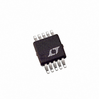
LTC1407CMSE-1#TRPBF Linear Technology, LTC1407CMSE-1#TRPBF Datasheet - Page 15

LTC1407CMSE-1#TRPBF
Manufacturer Part Number
LTC1407CMSE-1#TRPBF
Description
IC ADC 12BIT 3MSPS SAMPLE 10MSOP
Manufacturer
Linear Technology
Datasheet
1.LTC1407CMSE-1PBF.pdf
(26 pages)
Specifications of LTC1407CMSE-1#TRPBF
Number Of Bits
12
Sampling Rate (per Second)
3M
Data Interface
Serial, SPI™
Number Of Converters
1
Power Dissipation (max)
14mW
Voltage Supply Source
Single Supply
Operating Temperature
0°C ~ 70°C
Mounting Type
Surface Mount
Package / Case
10-TFSOP, 10-MSOP (0.118", 3.00mm Width) Exposed Pad
Lead Free Status / RoHS Status
Lead free / RoHS Compliant
Available stocks
Company
Part Number
Manufacturer
Quantity
Price
APPLICATIONS INFORMATION
INTERNAL REFERENCE
The LTC1407-1/LTC1407A-1 have an on-chip, temperature
compensated, bandgap reference that is factory trimmed
near 2.5V to obtain a precise ±1.25V input span. The ref-
erence amplifi er output V
with a capacitor to ground. The reference amplifier is
stable with capacitors of 1μF or greater. For the best noise
performance, a 10μF ceramic or a 10μF tantalum in paral-
lel with a 0.1μF ceramic is recommended. The V
can be overdriven with an external reference as shown
in Figure 3. The voltage of the external reference must be
higher than the 2.5V of the open-drain P-channel output
of the internal reference. The recommended range for an
external reference is 2.55V to V
at 2.55V will see a DC quiescent load of 0.75mA and as
much as 3mA during conversion.
INPUT SPAN VERSUS REFERENCE VOLTAGE
The differential input range has a unipolar voltage span that
equals the difference between the voltage at the reference
buffer output V
Pad ground. The differential input range of ADC is –1.25V
to 1.25V when using the internal reference. The internal
ADC is referenced to these two nodes. This relationship
also holds true with an external reference.
DIFFERENTIAL INPUTS
The ADC will always convert the bipolar difference of CH0
minus CH0
independent of the common mode voltage at either set
of inputs. The common mode rejection holds up at high
frequencies (see Figure 4). The only requirement is that
both inputs not go below ground or exceed V
nonlinearity errors (INL) and differential nonlinearity
–
or the bipolar difference of CH1
3V REF
REF
(Pin 3) and the voltage at the Exposed
Figure 3
REF
10μF
, (Pin 3) must be bypassed
11
DD
3
. An external reference
V
GND
REF
LTC1407A-1
LTC1407-1/
14071 F02
+
minus CH1
DD
. Integral
REF
pin
–
+
,
errors (DNL) are largely independent of the common
mode voltage. However, the offset error will vary. CMRR
is typically better than 60dB.
Figure 5 shows the ideal input/output characteristics for
the LTC1407-1/LTC1407A-1. The code transitions occur
midway between successive integer LSB values (i.e.,
0.5LSB, 1.5LSB, 2.5LSB, FS – 1.5LSB). The output code
is 2’s complement with 1LSB = 2.5V/16384 = 153μV for
the LTC1407A-1 and 1LSB = 2.5V/4096 = 610μV for the
LTC1407-1. The LTC1407A-1 has 1LSB RMS of Gaussian
white noise. Figure 6a shows the LTC1819 converting a
single-ended input signal to differential input signals for
optimum THD and SFDR performance as shown in the
FFT plot (Figure 6b).
Figure 5. LTC1407-1/LTC1407A-1 Transfer Characteristic
011...111
011...110
011...101
100...010
100...001
100...000
LTC1407-1/LTC1407A-1
–100
–120
–20
–40
–60
–80
0
–FS
100
Figure 4. CMRR vs Frequency
1k
INPUT VOLTAGE (V)
10k
FREQUENCY (Hz)
CH0
100k
1M
CH1
10M
FS – 1LSB
14071 F05
14071 F04
100M
15
14071fb


