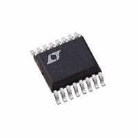
LTC2410CGN Linear Technology, LTC2410CGN Datasheet - Page 30

LTC2410CGN
Manufacturer Part Number
LTC2410CGN
Description
IC ADC 24BIT DIFF INP/REF 16SSOP
Manufacturer
Linear Technology
Datasheet
1.LTC2410CGNPBF.pdf
(48 pages)
Specifications of LTC2410CGN
Number Of Bits
24
Sampling Rate (per Second)
7.5
Data Interface
MICROWIRE™, Serial, SPI™
Number Of Converters
2
Power Dissipation (max)
1mW
Voltage Supply Source
Single Supply
Operating Temperature
0°C ~ 70°C
Mounting Type
Surface Mount
Package / Case
16-SSOP (0.150", 3.90mm Width)
Lead Free Status / RoHS Status
Contains lead / RoHS non-compliant
Other names
Q894257
Available stocks
Company
Part Number
Manufacturer
Quantity
Price
Part Number:
LTC2410CGN
Manufacturer:
LINEAR/凌特
Quantity:
20 000
Part Number:
LTC2410CGN#PBF
Manufacturer:
LINEAR/凌特
Quantity:
20 000
Part Number:
LTC2410CGN-1
Manufacturer:
LINEAR/凌特
Quantity:
20 000
APPLICATIO S I FOR ATIO
LTC2410
ity. Typical measured performance curves for output data
rates up to 100 readings per second are shown in Fig-
ures 27, 28, 29, 30, 31, 32, 33 and 34. In order to obtain
the highest possible level of accuracy from this converter
at output data rates above 20 readings per second, the
user is advised to maximize the power supply voltage used
and to limit the maximum ambient operating temperature.
In certain circumstances, a reduction of the differential
reference voltage may be beneficial.
Input Bandwidth
The combined effect of the internal Sinc
of the analog and digital autocalibration circuits deter-
mines the LTC2410 input bandwidth. When the internal
oscillator is used with the notch set at 60Hz (F
the 3dB input bandwidth is 3.63Hz. When the internal
oscillator is used with the notch set at 50Hz (F
the 3dB input bandwidth is 3.02Hz. If an external conver-
sion clock generator of frequency f
F
Due to the complex filtering and calibration algorithms
utilized, the converter input bandwidth is not modeled very
accurately by a first order filter with the pole located at the
3dB frequency. When the internal oscillator is used, the
shape of the LTC2410 input bandwidth is shown in Fig-
ure 35 for F
oscillator of frequency f
LTC2410 input bandwidth can be derived from Figure 35,
F
f
The conversion noise (800nV
can be modeled by a white noise source connected to a
noise free converter. The noise spectral density is
62.75nV Hz for an infinite bandwidth source and
86.1nV Hz for a single 0.5MHz pole source. From these
numbers, it is clear that particular attention must be given
to the design of external amplification circuits. Such
circuits face the simultaneous requirements of very low
bandwidth (just a few Hz) in order to reduce the output
referred noise and relatively high bandwidth (at least
500kHz) necessary to drive the input switched-capacitor
network. A possible solution is a high gain, low bandwidth
amplifier stage followed by a high bandwidth unity-gain
buffer.
30
EOSC
O
O
pin, the 3dB input bandwidth is 0.236 • 10
= LOW curve in which the horizontal axis is scaled by
/153600.
O
= LOW and F
U
EOSC
U
O
= HIGH. When an external
RMS
is used, the shape of the
EOSC
typical for V
W
is connected to the
4
digital filter and
–6
O
O
U
REF
= HIGH),
= LOW),
• f
EOSC
= 5V)
.
Figure 27. Offset Error vs Output Data Rate and Temperature
Figure 28. +FS Error vs Output Data Rate and Temperature
Figure 29. –FS Error vs Output Data Rate and Temperature
–1000
–2000
–3000
–4000
–5000
–6000
–7000
7000
6000
5000
4000
3000
2000
1000
500
450
400
350
300
250
200
150
100
50
0
0
0
0
0
0
V
REF
REF
V
V
F
10 20 30 40 50 60 70 80 90 100
V
REF
REF
IN
IN
F
10 20 30 40 50 60 70 80 90 100
V
REF
REF
IN
IN
F
OUTPUT DATA RATE (READINGS/SEC)
OUTPUT DATA RATE (READINGS/SEC)
10 20 30 40 50 60 70 80 90 100
O
O
CC
INCM
IN
CC
OUTPUT DATA RATE (READINGS/SEC)
O
CC
+
–
= EXTERNAL OSCILLATOR
= EXTERNAL OSCILLATOR
+
–
= EXTERNAL OSCILLATOR
+
= 0V
+
–
–
= 3.75V
= 1.25V
= 5V
= 5V
+
–
= 1.25V
= 3.75V
= 5V
= 5V
= 5V
= GND
= GND
= 5V
= GND
= 2.5V
T
A
= 25 C
T
A
T
= 85 C
T
A
A
T
= 25 C
= 25 C
A
T
A
= 85 C
= 85 C
2410 F27
2410 F28
2410 F29


