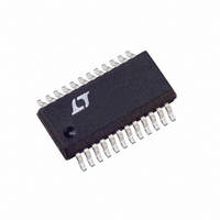
LTC1598LCG#TRPBF Linear Technology, LTC1598LCG#TRPBF Datasheet - Page 12

LTC1598LCG#TRPBF
Manufacturer Part Number
LTC1598LCG#TRPBF
Description
IC A/D CONV 12BIT SRL 8CH 24SSOP
Manufacturer
Linear Technology
Datasheet
1.LTC1598LCGPBF.pdf
(24 pages)
Specifications of LTC1598LCG#TRPBF
Number Of Bits
12
Sampling Rate (per Second)
10.5k
Data Interface
MICROWIRE™, QSPI™, Serial, SPI™
Number Of Converters
1
Power Dissipation (max)
480µW
Voltage Supply Source
Single Supply
Operating Temperature
0°C ~ 70°C
Mounting Type
Surface Mount
Package / Case
24-SSOP (0.200", 5.30mm Width)
Lead Free Status / RoHS Status
Lead free / RoHS Compliant
Available stocks
Company
Part Number
Manufacturer
Quantity
Price
APPLICATIONS
LTC1594L/LTC1598L
after a delay of t
ensure a break-before-make interval. After this interval,
the selected channel is switched on allowing signal
transmission. The selected channel remains on until the
next falling edge of CS and the process repeats itself with
the “EN” bit being logic high. If the “EN” bit is logic low,
all the channels are switched off simultaneously after a
delay of t
channels remain off until the next falling edge of CS.
Input Data Word
When CS is high, the LTC1594L/LTC1598L clock data
into the D
store the data into a 4-bit register. The input data words
are defined as follows:
“EN” Bit
The first bit in the 4-bit register is an “EN” bit. If the “EN”
bit is a logic high, as illustrated in Figure 1, it enables the
selected channel after a delay of t
low. If the “EN” bit is logic low, as illustrated in Figure 2,
it disables all channels after a delay of t
is pulled low.
Multiplexer (MUX) Address
The 3 bits of input word following the “EN” bit select the
channel in the MUX for the requested conversion. For a
given channel selection, the converter will measure the
voltage of the selected channel with respect to the voltage
on the COM pin. Tables 1 and 2 show the various bit
combinations for the LTC1594L/LTC1598L channel
selection.
Table 1. Logic Table for the LTC1594L Channel Selection
12
CHANNEL STATUS
All Off
CH0
CH1
CH2
CH3
IN
OFF
inputs on the rising edge of the clock and
from CS being pulled low and all the
OFF
U
, all the channels are switched off to
EN
EN
0
1
1
1
1
CHANNEL SELECTION
INFORMATION
D2
U
D2
D1
X
0
0
0
0
ON
1594L/98L AI02
D0
W
when the CS is pulled
D1
OFF
X
0
0
1
1
when the CS
U
DO
X
0
1
0
1
Table 2. Logic Table for the LTC1598L Channel Selection
Transfer Curve
The LTC1594L/LTC1598L are permanently configured
for unipolar only. The input span and code assignment
for this conversion type is illustrated below.
1 1 1 1 1 1 1 1 1 1 1 0
0 0 0 0 0 0 0 0 0 0 0 1
0 0 0 0 0 0 0 0 0 0 0 0
CHANNEL STATUS
1 1 1 1 1 1 1 1 1 1 1 1
All Off
CH0
CH1
CH2
CH3
CH4
CH5
CH6
CH7
1 1 1 1 1 1 1 1 1 1 1 1 1 1
1 1 1 1 1 1 1 1 1 1 1 1 1 0
0 0 0 0 0 0 0 0 0 0 0 0 0 1
0 0 0 0 0 0 0 0 0 0 0 0 0 0
•
•
•
OUTPUT CODE
•
•
•
EN
0
1
1
1
1
1
1
1
1
Transfer Curve
Output Code
INPUT VOLTAGE
V
V
REF
REF
1LSB =
1LSB
D2
0V
– 1LSB
– 2LSB
X
0
0
0
0
1
1
1
1
•
•
•
V
4096
REF
INPUT VOLTAGE
(V
D1
REF
X
0
0
1
1
0
0
1
1
2.49939V
2.49878V
0.00061V
= 2.500V)
0V
•
•
•
1594L/98L • AI04
1594L/98L • AI03
DO
X
0
1
0
1
0
1
0
1
15948lfb
V
IN


