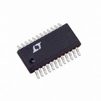
LTC1598LCG#TRPBF Linear Technology, LTC1598LCG#TRPBF Datasheet - Page 15

LTC1598LCG#TRPBF
Manufacturer Part Number
LTC1598LCG#TRPBF
Description
IC A/D CONV 12BIT SRL 8CH 24SSOP
Manufacturer
Linear Technology
Datasheet
1.LTC1598LCGPBF.pdf
(24 pages)
Specifications of LTC1598LCG#TRPBF
Number Of Bits
12
Sampling Rate (per Second)
10.5k
Data Interface
MICROWIRE™, QSPI™, Serial, SPI™
Number Of Converters
1
Power Dissipation (max)
480µW
Voltage Supply Source
Single Supply
Operating Temperature
0°C ~ 70°C
Mounting Type
Surface Mount
Package / Case
24-SSOP (0.200", 5.30mm Width)
Lead Free Status / RoHS Status
Lead free / RoHS Compliant
Available stocks
Company
Part Number
Manufacturer
Quantity
Price
APPLICATIONS
BOARD LAYOUT CONSIDERATIONS
Grounding and Bypassing
The LTC1594L/LTC1598L are easy to use if some care is
taken. They should be used with an analog ground plane
and single point grounding techniques. The GND pin
should be tied directly to the ground plane.
The V
a 10 F tantalum capacitor with leads as short as possible.
If the power supply is clean, the LTC1594L/LTC1598L
can also operate with smaller 1 F or less surface mount
or ceramic bypass capacitors. All analog inputs should
be referenced directly to the single point ground. Digital
inputs and outputs should be shielded from and/or
routed away from the reference and analog circuitry.
CSADC = CSMUX = CS
CC
MUXOUT = ADCIN
pin should be bypassed to the ground plane with
CH0 TO CH7
D
COM
CLK
OUT
D
IN
U
INFORMATION
U
Figure 7. LTC1594L/LTC1598L ADCIN and COM Input Settling Windows
EN
W
D2
U
D1
SAMPLE-AND-HOLD
Both the LTC1594L/LTC1598L provide a built-in sample-
and-hold (S&H) function to acquire signals through the
selected channel, assuming the ADCIN and MUXOUT
pins are tied together. The S & H of these parts acquire
input signals through the selected channel relative to
COM input during the t
Single-Ended Inputs
The sample-and-hold of the LTC1594L/LTC1598L allows
conversion of rapidly varying signals. The input voltage
is sampled during the t
The sampling interval begins after t
is pulled low and continues until the second falling CLK
edge after the CS is low (see Figure 7). On this falling CLK
D0
t
ON
1ST BIT TEST “COM” INPUT MUST
SAMPLE
SETTLE DURING THIS TIME
“ANALOG” INPUT MUST
SETTLE DURING
THIS TIME
t
SMPL
LTC1594L/LTC1598L
SMPL
SMPL
time (see Figure 7).
time as shown in Figure 7.
HOLD
DON‘T CARE
ON
t
CONV
time once the CS
1594L/98L F07
B11
15
15948lfb


