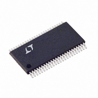
LTC1852IFW#PBF Linear Technology, LTC1852IFW#PBF Datasheet - Page 3

LTC1852IFW#PBF
Manufacturer Part Number
LTC1852IFW#PBF
Description
IC A/D CONV 8CH 10BIT 48-TSSOP
Manufacturer
Linear Technology
Datasheet
1.LTC1853CFWPBF.pdf
(24 pages)
Specifications of LTC1852IFW#PBF
Number Of Bits
10
Sampling Rate (per Second)
400k
Data Interface
Parallel
Number Of Converters
1
Power Dissipation (max)
15mW
Voltage Supply Source
Single Supply
Operating Temperature
-40°C ~ 85°C
Mounting Type
Surface Mount
Package / Case
48-TFSOP (0.240", 6.10mm Width)
Lead Free Status / RoHS Status
Lead free / RoHS Compliant
Available stocks
Company
Part Number
Manufacturer
Quantity
Price
temperature range, otherwise specifi cations are at T
Resolution (No Missing Codes)
Integral Linearity Error
Differential Linearity Error
Offset Error (Bipolar and Unipolar)
Offset Error Match (Bipolar and Unipolar)
Unipolar Gain Error
Unipolar Gain Error Match
Bipolar Gain Error Match
Bipolar Gain Error
Full-Scale Error Temperature Coeffi cient
specifi cations are at T
SYMBOL
V
I
C
t
t
t
t
CMRR
SYMBOL
S/(N + D)
THD
SFDR
CONVERTER CHARACTERISTICS
ANALOG INPUT
DYNAMIC ACCURACY
Bipolar Gain Error
Unipolar Gain Error
IN
ACQ
S(MUX)
AP
jitter
PARAMETER
IN
IN
Gain = 1 (PGA = 1)
Gain = 2 (PGA = 0)
Gain = 1 (PGA = 1)
Gain = 2 (PGA = 0)
Gain = 1 (PGA = 1)
Gain = 2 (PGA = 0)
Gain = 1 (PGA = 1)
Gain = 2 (PGA = 0)
Gain = 1 (PGA = 1)
Gain = 2 (PGA = 0)
PARAMETER
Analog Input Range (Note 9)
Unipolar, Gain = 1 (PGA = 1)
Unipolar, Gain = 2 (PGA = 0)
Bipolar, Gain = 1 (PGA = 1)
Bipolar, Gain = 2 (PGA = 0)
Analog Input Leakage Current
Analog Input Capacitance
Sample-and-Hold Acquisition Time
Multiplexer Settling Time (Includes t
Sample-and-Hold Aperture Delay Time
Sample-and-Hold Aperture Delay Time Jitter
Analog Input Common Mode Rejection Ratio
PARAMETER
Signal-to-Noise Plus Distortion Ratio
Total Harmonic Distortion
Spurious Free Dynamic Range
A
= 25°C. (Notes 5)
The
l
CONDITIONS
(Note 7)
(Note 8)
REFCOMP ≥ 2V
With External 4.096V Reference
Applied to REFCOMP (Note 12)
V
With External 4.096V Reference
Applied to REFCOMP (Note 12)
V
With External 2.5V Reference
Applied to REFCOMP
V
With External 2.5V Reference
Applied to REFCOMP
V
denotes the specifi cations which apply over the full operating temperature range, otherwise
DD
DD
DD
DD
T
= 4.75V to 5.25V, f
= 4.75V to 5.25V, f
= 2.7V to 5.5V, f
= 2.7V to 5.5V, f
ACQ
A
= 25°C. (Notes 5)
)
A
CONDITIONS
2.7V ≤ V
Between Conversions (Gain = 1)
Between Conversions (Gain = 2)
During Conversions
V
V
CONDITIONS
40kHz Input Signal
40kHz Input Signal, First 5 Harmonics
40kHz Input Signal
= 25°C. V
DD
DD
S
S
= 5V
= 5V
≤ 250kHz
≤ 250kHz
S
S
The
≤ 400kHz
≤ 400kHz
DD
DD
≤ 5.5V, REFCOMP ≤ V
l
denotes the specifi cations which apply over the full operating
= 2.7V to 5.5V, REFCOMP < V
l
l
l
l
l
l
l
l
l
MIN
10
DD
LTC1852
±0.25
±0.25
±0.5
TYP
±1
±1
±2
±1
±2
15
l
LTC1852/LTC1853
MAX
±0.5
±0.5
±0.5
DD
±1
±1
±2
±4
±2
±4
±2
±4
±3
±6
±3
±6
MIN
MIN
(Notes 5,6)
0 – REFCOMP/2
0 – REFCOMP
± REFCOMP/2
±REFCOMP/4
MIN
12
– 0.5
72.5
–80
TYP
TYP
–85
15
25
50
50
60
5
2
LTC1853
±0.35
±0.25
±1.5
±1.5
TYP
±1
±2
±3
±3
15
MAX
MAX
150
150
±1
MAX
±12
±16
±16
±1
±1
±6
±1
±4
±8
±1
±4
±8
±1
±8
±8
ppm/°C
UNITS
UNITS
UNITS
ps
18523fa
3
LSB
LSB
LSB
LSB
LSB
LSB
LSB
LSB
LSB
LSB
LSB
LSB
LSB
LSB
LSB
Bits
RMS
μA
dB
dB
dB
dB
pF
pF
pF
ns
ns
ns
V
V
V
V


